Microfluidic Chips

Microfluidic chips are precision-fabricated microdevices containing integrated networks of microchannels designed for precise manipulation of small fluid volumes. These chips are manufactured from glass, polymethyl methacrylate (PMMA), silicon, quartz, or poly-dimethylsiloxane (PDMS) materials and can be custom etched to specific channel geometries and dimensions. With microchannel dimensions up to one hundred microns and fluid handling capabilities from 1 attolitre to one nanoliter, these devices enable automated, multiplexed analysis systems for biological, chemical, and diagnostic applications.
The integrated microchannel networks allow researchers to perform complex fluid manipulations including mixing, separation, routing, and analysis within a compact platform. These chips demonstrate resistance to high temperatures, pressures, and corrosion, making them suitable for demanding experimental conditions. Available in quantities of 5, 10, 15, or 30 units, with minimum feature sizes of 2 μm achievable using negative photoresist processing, these microfluidic platforms support applications ranging from single-cell analysis to organ-on-chip modeling and biomarker detection.
How It Works
Microfluidic chips operate on the principle of laminar flow within microscale channels, where fluid behavior is dominated by viscous forces rather than inertial forces due to the low Reynolds numbers. The integrated microchannel networks are precisely etched into the substrate material using photolithography and etching techniques, creating pathways that guide fluid flow through designed geometries. Fluids are introduced and withdrawn through access holes that connect the microchannel network to external pumps, syringes, or pressure systems.
The small channel dimensions enable precise control over fluid mixing, separation, and reaction conditions through controlled diffusion and interface formation. Multiple fluid streams can be combined, split, or manipulated within the same chip platform, allowing for complex analytical procedures to be automated and miniaturized. The high surface-area-to-volume ratio within the microchannels enhances mass transfer and reaction kinetics compared to conventional macroscale systems.
Custom etching capabilities allow for specific channel geometries tailored to experimental requirements, whether for cell trapping arrays, mixing chambers, reaction zones, or separation channels. The material properties of the chip substrate (glass, PMMA, silicon, quartz, or PDMS) determine chemical compatibility, optical transparency, and thermal characteristics suitable for different experimental conditions.
Features & Benefits
Microchannel Dimensions
- up to a hundred microns
Fluid Volume Handling
- 1 attolitre to one nano-liter
Minimum Feature Size Negative Pr
- 2 µm
Spreading Thickness Negative Pr
- 1-3 µm
Temperature Resistance
- high temperatures
Pressure Resistance
- high pressures
Corrosion Resistance
- yes
Custom Etching
- available to custom specifications
quantity
- 30
Automation Level
- manual
Material
- glass
- poly-dimethylsiloxane (PDMS)
- polymethyl methacrylate (PMMA)
- quartz
- silicon
Research Domain
- Analytical Chemistry
- Cancer Research
- Cell Biology
- Clinical Diagnostics
- Developmental Biology
- Immunology
- Materials Science
- Microbiology
- Pharmaceutical QC
Weight
- 4.41 lbs
Dimensions
- 65.0 × 36.0 × 27.0 cm
Product Highlights
| Feature | This Product | Category Context |
|---|---|---|
| Minimum Feature Size | 2 μm achievable with negative photoresist | Standard devices often limited to 10-50 μm features |
| Substrate Material Options | Five materials available: glass, PMMA, silicon, quartz, PDMS | Most vendors offer 1-2 standard materials |
| Volume Range | Handles 1 attolitre to 1 nanoliter | Many devices limited to picoliter to microliter range |
| Custom Design Capability | Full custom etching to specifications | Fixed channel patterns with limited customization |
| Quantity Flexibility | Available in 5, 10, 15, or 30 unit quantities | Often requires minimum orders of 100+ units for custom work |
| Temperature Resistance | High temperature resistance across all materials | Limited thermal stability in polymer-based devices |
These microfluidic chips provide exceptional design flexibility with custom etching capabilities down to 2 μm features across five substrate materials. The ultra-low volume handling capabilities and availability in small quantities make them ideal for specialized research applications requiring precise fluid control.
Applications & Use Cases
Practical Tips
Always prime channels slowly with degassed fluids to prevent bubble formation in narrow passages.
Air bubbles can block channels and disrupt flow patterns in microfluidic systems
Flush channels with appropriate cleaning solvents immediately after use to prevent protein or particle buildup.
Residue accumulation can alter channel dimensions and affect flow characteristics
Verify flow rates using fluorescent tracers or microsphere standards before critical experiments.
Small fabrication variations can significantly impact flow behavior in microscale channels
Handle glass and silicon chips with appropriate tools to prevent injury from sharp edges.
Microfluidic substrates can be fragile and may create sharp fragments if broken
Document all flow parameters, pressures, and environmental conditions for each experiment.
Microfluidic experiments are sensitive to operating conditions and require detailed records for reproducibility
Use microscopy to inspect channel integrity if unexpected flow behavior occurs.
Microscopic cracks or debris may not be visible to the naked eye but can significantly affect performance
Store unused chips in protective packaging in a clean, dry environment.
Contamination or moisture can affect surface properties and channel performance
Replace tubing connections regularly as repeated use can degrade fitting integrity.
Leaky connections can introduce pressure variations and affect experimental reproducibility
Setup & Operation Guide
-
Unpack and InspectRemove microfluidic chips from packaging and inspect for cracks, debris, or channel blockages using a microscope. Verify channel integrity and access hole clarity.
-
Surface PreparationClean chip surfaces with appropriate solvents based on substrate material (isopropanol for glass/PMMA, gentle detergent for PDMS). Ensure complete removal of fabrication residues.
-
Interface AssemblyConnect tubing and fittings to access holes using appropriate connectors for your fluid delivery system. Verify leak-free connections at operating pressures.
-
System PrimingFill channels with appropriate buffer or carrier fluid to remove air bubbles and establish stable flow conditions. Use low flow rates initially to prevent channel damage.
-
Flow VerificationTest fluid flow through all channels using colored dyes or microsphere suspensions to verify proper channel function and identify any blockages or leaks.
-
Operational TestingPerform initial functionality tests with sample fluids at target flow rates and pressures to confirm system performance meets experimental requirements.
-
Protocol ImplementationBegin experimental protocols with proper flow control and monitoring systems in place. Document flow rates, pressures, and system performance for reproducibility.
What's in the Box
- Microfluidic chips (quantity as specified: 5, 10, 15, or 30 units)
- Protective chip holders or carriers (typical)
- Handling instructions and protocols (typical)
- Material specification documentation (typical)
- Quality control certificates (typical)
Warranty & Support
ConductScience provides a standard manufacturer warranty covering defects in materials and workmanship. Technical support is available for fabrication specifications and application guidance.
Compliance & Standards
Background Reading
The following papers provide general scientific background on measurement techniques relevant to this product category. They are not validation studies of this specific instrument.
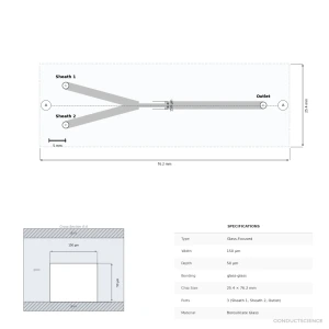
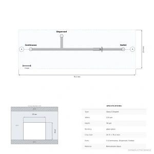
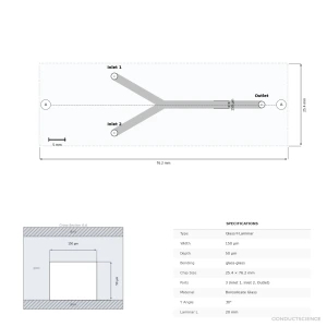
What channel geometries can be fabricated with custom etching?
Custom etching allows for a wide range of channel geometries including straight channels, serpentine patterns, branching networks, mixing chambers, and specialized structures like cell traps or droplet generators, with minimum feature sizes of 2 μm.
How do I select the appropriate substrate material for my application?
Glass offers excellent chemical resistance and optical clarity for microscopy, PMMA provides good optical properties at lower cost, silicon enables electronic integration, quartz offers superior chemical inertness, and PDMS allows for flexible bonding and gas permeability.
What flow rates and pressures are compatible with these chips?
Operating parameters depend on channel geometry and substrate material, but the high temperature and pressure resistance specifications suggest compatibility with typical microfluidic flow rates from nL/min to μL/min and pressures up to several bar.
Can these chips be reused for multiple experiments?
Reusability depends on the substrate material and experimental conditions. Glass and silicon chips can often be cleaned and reused, while PDMS chips may have limited reuse due to material properties and potential contamination issues.
What fabrication tolerances should I expect for custom designs?
With minimum feature sizes of 2 μm achievable and negative photoresist spreading thickness of 1-3 μm, fabrication tolerances are typically within ±1-2 μm for critical dimensions, though specific tolerances should be confirmed with design specifications.
How do these chips compare to other microfluidic platforms?
These custom-etched chips offer greater design flexibility compared to standard microfluidic devices, with multiple material options and precise dimensional control, making them suitable for specialized applications requiring specific channel geometries.
What surface treatments are available for the channels?
Surface treatments vary by substrate material and can include plasma treatment, silanization, or polymer coatings to modify surface properties for specific applications such as cell adhesion, protein adsorption, or wetting characteristics.
What is the typical lead time for custom chip fabrication?
Lead times depend on design complexity and fabrication processes required, but custom etching typically requires several weeks from design finalization to delivery, particularly for complex geometries or specialized materials.
Have a question about this product?
Frequently Bought Together


Related Products