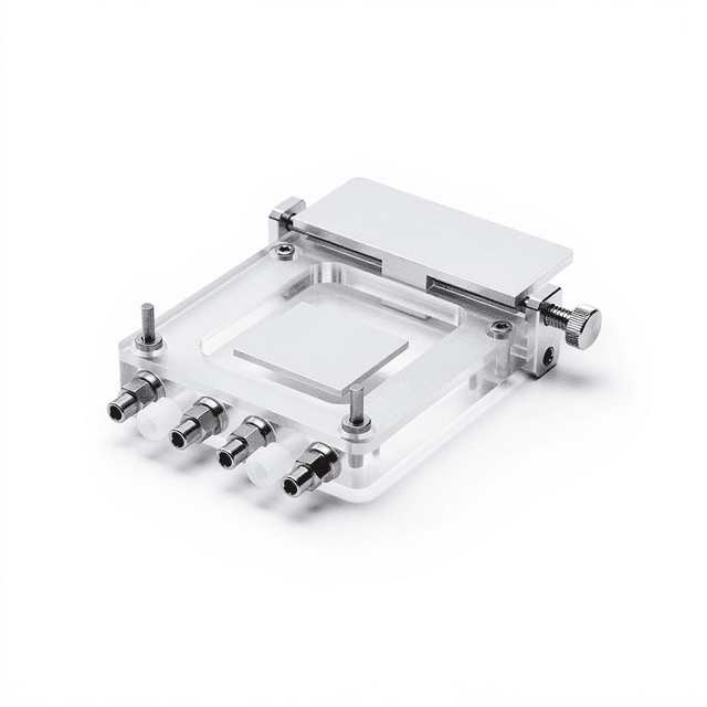
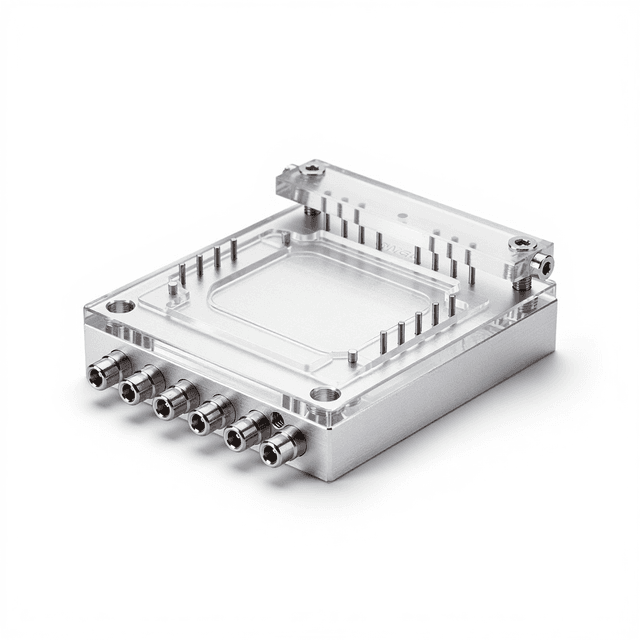
Silicon Microfluidic Chip
Silicon microfluidic chip fabricated using DRIE technology for high-aspect-ratio channel applications and thermal management in lab-on-chip systems.
Reusable chip — designed for multiple experimental runs. Compatible with standard microfluidic tubing: steel pins (0.7 mm ID / 1.0 mm OD) and silicone tubing (0.8 mm ID / 1.9 mm OD). Available in bulk packs (5‑, 10‑, and 25‑unit) for lab-scale and consumable workflows.

Louise Corscadden, PhD
Director of Science · ConductScience
Ask Louise about Silicon Microfluidic Chip fit, setup, configuration, or quote prep.
Already working with us? Sign in to connect this with My Scientist.
Key Specifications
Full details →- Model fit
- 3 selectable configurations
- SKU family
- WHM-0026
- Sizing
- 25.0 x 15.0 x 1.0 cm
- Ordering
- Online checkout and quote request available
- Category
- Lab Equipment
- Build notes
- Confirm accessories, station layout, and support needs before purchase
This silicon microfluidic chip utilizes Deep Reactive Ion Etching (DRIE) fabrication to create precise microstructures for microfluidic applications. The 25mm x 15mm x 1mm silicon substrate provides a stable platform for creating high-aspect-ratio channels and implementing thermal management solutions in lab-on-chip systems.
The DRIE fabrication process enables the creation of vertical sidewalls and deep features with high precision, making this chip suitable for applications requiring controlled fluid flow, precise channel geometries, and effective heat dissipation. The silicon material offers excellent thermal conductivity and chemical compatibility for a wide range of analytical and research applications.
How It Works
The silicon microfluidic chip operates through precisely etched microchannels created using Deep Reactive Ion Etching (DRIE) technology. DRIE alternates between etching and passivation steps to create vertical sidewalls with minimal undercutting, enabling high-aspect-ratio features with excellent dimensional control.
The silicon substrate provides superior thermal conductivity (150 W/m·K) compared to polymer alternatives, enabling effective heat dissipation and temperature uniformity across the chip surface. This thermal management capability is critical for temperature-sensitive applications and processes requiring precise thermal control.
Fluid flow through the microchannels is governed by laminar flow principles at the microscale, with Reynolds numbers typically below 1. The high-aspect-ratio geometry maximizes surface-to-volume ratios while maintaining predictable flow characteristics for reproducible experimental conditions.
Features & Benefits
Pack Size
- 5-Pack
- 10-Pack
- 25-Pack
Weight
- 0.02 kg
Dimensions
- L: 25.0 mm
- W: 15.0 mm
- H: 1.0 mm
| Feature | This Product | Typical Alternative | Advantage |
|---|---|---|---|
| Material Platform | Silicon with DRIE fabrication | PDMS polymer chips are common for prototyping applications | Provides superior thermal conductivity and chemical resistance for demanding analytical applications. |
| Fabrication Method | Deep Reactive Ion Etching (DRIE) | Soft lithography methods typically offer lower resolution | Enables high-aspect-ratio features with vertical sidewalls and precise dimensional control. |
| Thermal Management | Optimized for thermal management applications | Polymer chips often have limited thermal conductivity | Critical for temperature-sensitive experiments and applications requiring precise thermal control. |
| Channel Geometry | High-aspect-ratio channel capability | Standard chips often have lower aspect ratio limitations | Maximizes surface-to-volume ratios for enhanced reaction efficiency and separation performance. |
| Form Factor | 25mm x 15mm x 1mm compact design | Varies by model and application requirements | Provides optimal balance between functional area and compatibility with standard laboratory equipment. |
This silicon microfluidic chip leverages DRIE fabrication technology to provide high-aspect-ratio channels with excellent thermal management capabilities. The silicon platform offers superior chemical resistance and thermal properties compared to polymer alternatives, making it suitable for demanding analytical and research applications.
| Model | SKU | Listed price | Status | Dimensions |
|---|---|---|---|---|
| 25-Pack | WHM-0026-25PK | Quote | Available | 25.0 x 15.0 x 1.0 cm |
| 10-Pack | WHM-0026-10PK | $1,490.00 | Available | 25.0 x 15.0 x 1.0 cm |
| 5-Pack | WHM-0026-5PK | Quote | Available | 25.0 x 15.0 x 1.0 cm |
Practical Tips
Store chips in clean, dry environment and handle with appropriate tools to prevent surface contamination and physical damage.
Why: Silicon surfaces are sensitive to particulate contamination which can affect channel performance.
Implement regular cleaning cycles with compatible solvents and verify channel integrity under microscope after each use.
Why: Prevents accumulation of residues that could alter flow characteristics or block channels.
Verify flow rates and pressure distributions periodically using traceable flow measurement standards.
Why: Ensures consistent experimental conditions and validates system performance over time.
Document environmental conditions including temperature and humidity during experiments for reproducible results.
Why: Silicon thermal properties can be affected by ambient conditions, influencing experimental outcomes.
If channels appear blocked, use appropriate organic solvents or plasma cleaning before applying higher pressures.
Why: Prevents damage to channel structures while effectively removing most common contaminants.
Use appropriate personal protective equipment when handling cleaning solvents and follow established chemical safety protocols.
Why: Silicon chips may require aggressive cleaning agents that pose health and safety risks.
Setup Guide
What’s in the Box
- Silicon microfluidic chip
- Protective storage container (typical)
- Technical specification sheet (typical)
- Handling guidelines documentation (typical)
Warranty
ConductScience provides a standard one-year manufacturer warranty covering material defects and fabrication quality. Technical support is available for integration guidance and application-specific questions.
Compliance
References
Background reading relevant to this product:
What channel dimensions can be achieved with DRIE fabrication?
DRIE fabrication enables channel widths from 10 micrometers to several millimeters with aspect ratios up to 20:1. Specific dimensions depend on design requirements and should be confirmed during the design phase.
How does silicon thermal conductivity affect experimental temperature control?
Silicon's high thermal conductivity (150 W/m·K) provides rapid thermal equilibration and uniform temperature distribution, critical for temperature-sensitive assays and thermal cycling applications.
What surface treatments are compatible with silicon microfluidic chips?
Silicon surfaces can be functionalized with silane chemistry, plasma treatments, or thin film coatings to modify surface properties for specific applications. Consult product datasheet for recommended protocols.
What pressure limits should be considered for channel operation?
Operating pressure limits depend on channel geometry and bonding method. Typical silicon chips can withstand pressures up to several bar, but specific limits should be verified for each design.
How do I prevent clogging in high-aspect-ratio channels?
Use appropriate filtration upstream, maintain proper flow rates, and implement regular cleaning protocols with compatible solvents to prevent particle accumulation and biofilm formation.
Can the chip be reused for multiple experiments?
Yes, with proper cleaning protocols between uses. Silicon is chemically inert and can withstand most organic solvents and mild acids/bases for thorough decontamination.
What optical compatibility does the 1mm thickness provide?
The 1mm thickness is compatible with standard microscope objectives and allows for both transmitted and reflected light microscopy with working distances suitable for most imaging applications.
Have a question about this product?
Have a question? Just ask.
Send it over and we'll email you a personalized answer — no call, no scheduling.
Prefer to talk it through?
Accessories
Enhance your setup with compatible accessories