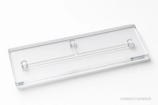
PDMS Chip (PMMA Mold Process)
Cost-effective PDMS microfluidic chip fabricated using CNC-machined PMMA molds, featuring minimum channel dimensions greater than 50 micrometers for cell culture and droplet generation applications.
Reusable chip — designed for multiple experimental runs. Compatible with standard microfluidic tubing: steel pins (0.7 mm ID / 1.0 mm OD) and silicone tubing (0.8 mm ID / 1.9 mm OD). Available in bulk packs (5‑, 10‑, and 25‑unit) for lab-scale and consumable workflows.

Louise Corscadden, PhD
Director of Science · ConductScience
Ask Louise about PDMS Chip (PMMA Mold Process) fit, setup, configuration, or quote prep.
Already working with us? Sign in to connect this with My Scientist.
Key Specifications
Full details →- Model fit
- 2 selectable configurations
- SKU family
- WHM-0129
- Sizing
- 181.8 x 136.3 x 90.9 cm
- Ordering
- Online checkout and quote request available
- Category
- Microfluidic Chips
- Build notes
- Confirm accessories, station layout, and support needs before purchase
The PDMS Chip (PMMA Mold Process) is a polydimethylsiloxane-based microfluidic device fabricated using CNC-machined PMMA master molds. This manufacturing approach enables cost-effective production of microfluidic chips with minimum feature sizes greater than 50 micrometers, making it suitable for applications requiring larger microchannels without the precision demands of photolithographic processes.
The PMMA mold process offers an accessible alternative to traditional soft lithography techniques, allowing researchers to prototype and fabricate microfluidic devices for cell culture, droplet generation, and flow focusing applications. The elastomeric PDMS material provides the flexibility and biocompatibility required for biological microfluidics while maintaining compatibility with standard laboratory protocols and reagents.
How It Works
The PDMS chip fabrication process begins with CNC machining of PMMA master molds, where computer-controlled milling creates the desired channel geometries with minimum feature sizes exceeding 50 micrometers. This subtractive manufacturing approach enables rapid prototyping of microfluidic designs without requiring cleanroom facilities or photolithographic masks.
Liquid PDMS prepolymer is cast against the PMMA master mold and thermally cured to create the elastomeric microfluidic device. The cured PDMS chip is peeled from the mold, bonded to a substrate (typically glass or additional PDMS), and fitted with fluidic connections. The resulting device maintains the dimensional accuracy of the CNC-machined features while providing the chemical inertness and optical transparency required for microfluidic applications.
Fluid manipulation within the chip relies on precise control of flow rates and channel geometries to achieve laminar flow conditions. At the microscale, Reynolds numbers are typically low, allowing predictable fluid behavior for applications such as droplet generation through flow focusing or controlled mixing through diffusion-based processes.
Features & Benefits
Pack Size
- 10-Pack
- 25-Pack
Weight
- 3.3 kg
Dimensions
- L: 181.8 mm
- W: 136.3 mm
- H: 90.9 mm
| Feature | This Product | Typical Alternative | Advantage |
|---|---|---|---|
| Minimum Feature Size | Greater than 50 micrometers | Photolithographic methods can achieve sub-micrometer features but require specialized facilities | Larger features reduce clogging risk and enable simpler fabrication processes suitable for educational and prototype applications |
| Mold Fabrication Method | CNC-machined PMMA | Silicon wafer masters require cleanroom photolithography | Eliminates cleanroom requirements and enables rapid design iteration for prototyping applications |
| Material Composition | PDMS elastomer | Alternative materials include glass, thermoplastics, or paper-based substrates | Provides optimal biocompatibility and gas permeability for cell culture applications while maintaining cost-effectiveness |
| Production Cost Structure | Cost-effective manufacturing | High-resolution devices often require expensive mask sets and cleanroom processing | Enables economical production of multiple devices for screening studies and educational applications |
This PDMS chip offers accessible microfluidics fabrication through CNC-machined PMMA molds, prioritizing cost-effectiveness and rapid prototyping over ultra-high resolution features. The approach makes microfluidics technology available to laboratories without cleanroom facilities while maintaining the biocompatibility and optical properties required for biological applications.
| Model | SKU | Listed price | Status | Dimensions |
|---|---|---|---|---|
| 25-Pack | WHM-0129-25PK | Quote | Available | 181.8 x 136.3 x 90.9 cm |
| 10-Pack | WHM-0129-10PK | $1,490.00 | Available | 181.8 x 136.3 x 90.9 cm |
Practical Tips
Store PDMS chips in a dust-free environment and handle with clean tweezers to prevent particulate contamination of channels.
Why: Maintaining cleanliness prevents clogging and ensures reproducible experimental results.
Flush channels with appropriate cleaning solutions between uses and store filled with buffer to prevent air bubble formation.
Why: Regular cleaning prevents cross-contamination and maintains consistent flow characteristics.
Verify flow rates using tracer particles or dye solutions before critical experiments to ensure proper channel function.
Why: Flow rate verification confirms device integrity and enables accurate experimental parameter control.
If channels appear blocked, use gentle back-flushing with filtered solutions rather than excessive pressure that could damage the PDMS.
Why: PDMS elasticity limits pressure tolerance, and gentle methods preserve device integrity for continued use.
Allow adequate equilibration time after changing flow conditions to achieve stable laminar flow patterns.
Why: Flow stabilization ensures reproducible mixing and droplet generation characteristics critical for quantitative results.
Use appropriate personal protective equipment when handling organic solvents or biological samples in microfluidic devices.
Why: Microscale volumes can still present exposure risks, and proper safety protocols protect researchers and maintain sample integrity.
Setup Guide
What’s in the Box
- PDMS microfluidic chip (typical)
- Protective packaging (typical)
- Basic handling instructions (typical)
Warranty
ConductScience provides standard warranty coverage against manufacturing defects. Technical support is available for fabrication questions and application guidance.
Compliance
References
Background reading relevant to this product:
What is the minimum channel width achievable with the PMMA mold process?
The minimum feature size is greater than 50 micrometers due to the CNC machining limitations of PMMA master molds. For smaller features, photolithographic processes would be required.
How many devices can be produced from a single PMMA mold?
PMMA molds are reusable for multiple casting cycles. The exact number depends on mold care and the complexity of features, but typically dozens of chips can be produced from one master.
What surface treatments are compatible with these PDMS chips?
Standard PDMS surface modifications including plasma oxidation, silane treatments, and protein adsorption can be applied. Consult product datasheet for specific treatment protocols and compatibility.
Are these chips suitable for high-pressure applications?
PDMS has inherent flexibility that limits maximum operating pressure. The chip design and bonding method determine pressure limits; consult specifications for your specific application requirements.
Can the chips be sterilized for cell culture work?
PDMS chips can typically be sterilized using UV exposure, ethylene oxide, or autoclave methods. Verify compatibility with your specific sterilization protocol and cell culture requirements.
What optical properties does the PDMS material provide?
PDMS offers excellent optical transparency in the visible spectrum and is compatible with standard fluorescence microscopy. UV transmission varies with thickness and should be characterized for specific applications.
How do I prevent channel clogging during operation?
The 50+ micrometer minimum feature size reduces clogging risk compared to smaller channels. Use appropriate filtration of samples and maintain consistent flow rates to minimize particle accumulation.
Have a question about this product?
Have a question? Just ask.
Send it over and we'll email you a personalized answer — no call, no scheduling.
Prefer to talk it through?