Solder joint inspection
Joint-quality classification and void measurement for solder and bond images.
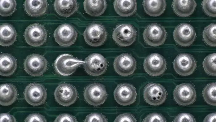
Example outputs shown for illustration. Numbers depend on your samples and protocol.
Results
Each measurement below comes from your own images, tied back to the annotated frame it came from, so results stay comparable across samples, locations, and conditions.
class
Joint class
Each detected feature assigned to a class using the agreed rule set, shown on the image.
Example, not a claimed result
In your report: Per-feature class, counts by class, and annotated overlays.
% area
Void %
Segmented area of the feature divided by the eligible area in the two-dimensional image.
Example, not a claimed result
In your report: Per-field value, size distribution, and the segmentation overlay used.
per area
Defect map
Findings placed in sample coordinates to reveal spatial patterns and local density.
In your report: Coordinate-referenced map, regional density, and representative images.
µm or count
Count
Size and shape measured for every detected object, then summarized across the population.
In your report: Per-object table, size distribution, and summary percentiles.
Built around your image set
Use the calibrated images your team already collects, together with the locations you need to compare.
Each report includes
The artifacts your team receives, ready for review and archive.
Annotated image set
Original images with regions of interest, measurement points, masks, and finding overlays.
Measurement table
Location-indexed values, units, distributions, and QC flags in a structured export.
Method record
Calibration evidence, analysis settings, version history, and validation summary.
Confidence in every resultTraceable measurements, reviewed against your agreed reference method.
- Traceable scale
- The report records the image scale, calibration evidence, and a method-specific expanded measurement uncertainty. It does not use one product-wide accuracy number.
- Reference comparison
- The configured method is compared with your accepted reference method or reviewed annotations, and reports bias by measurement range and image condition.
- Detection performance
- Detections are evaluated against reviewed reference regions with precision, recall, and segmentation overlap, separated by the conditions that affect performance.
- Repeatability
- The locked protocol is rerun on the same inputs and on a defined repeat set. The review records variation from image acquisition, sampling, and analysis separately where possible.
The measurement, today
Solder voids and joint defects are inspected manually, which is slow and misses sub-surface voids in BGA joints.
From image to reviewed result
- 1
Calibrate the scale
Set spatial scale from a bar or known dimension. Every downstream number inherits real units.
- 2
Detect & segment
Segmentation models find the objects and regions of interest: grains, particles, pores, fibers, cells.
- 3
Measure
Quantify size, count, area fraction, density, and orientation. The metrics your method already defines.
- 4
Review the overlay
Inspect the result on every field. Adjust thresholds by hand; the change is logged with the output.
- 5
Export & compare
Publication-ready statistics, plus batch comparison across lots, conditions, and time points.
Not sure this is the right measurement?
Send a representative image and your measurement goal. A ConductVision scientist will confirm whether this is the right fit, or point you to the closer workflow, before you commit to a quote.
Related applications
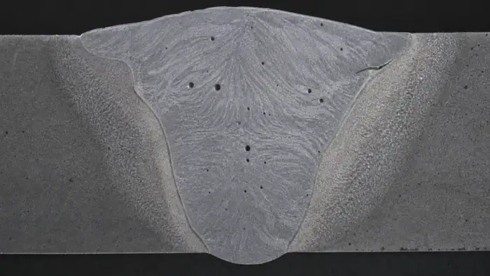
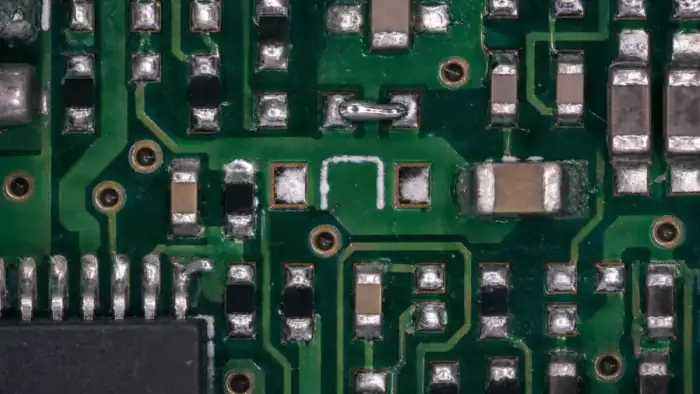
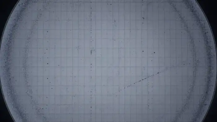
Send a sample image and a measurement goal
We will show the closest ConductVision workflow and flag what needs custom validation for your images.