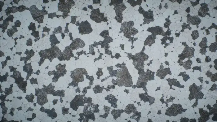
Materials vision software for measurement, inspection, and digital twins.
Connect microscopy, SEM, CT, macro imaging, and video inspection to calibrated measurements, reviewable overlays, batch exports, and digital-twin-ready material records.
- 34
- Applications across eight measurement families.
- 7+
- Standards referenced, from grain size to pilling.
- 10
- Shared primitives behind every page.
- 100%
- Outputs reviewable. Overlays and thresholds logged.
Measure the structures your lab already reviews by eye
Eight visual measurement families, one reviewable engine. Each routes into concrete applications for metals, coatings, powders, textiles, electronics, geology, and the life sciences.
Microstructure & metallography
Grains, phases, inclusions, and fracture surfaces from optical and SEM micrographs.
Surface, coating & corrosion
Coatings, films, corrosion, wear, and wettability across the surface-engineering stack.
Powder, particle & granular
Size, shape, and dispersion from micro to nano, for powders, catalysts, and minerals.
Textile, polymer & composite
Pilling, fibers, films, and inclusions for soft and fiber-reinforced materials.
Additive & advanced manufacturing
Powder to post-build, and the electrodes behind modern energy storage.
Joining, electronics & semiconductor
Welds, solder, wafers, and boards: defect class, density, and geometry.
Geology, minerals & porous
Pores, minerals, grains, and fractures from thin sections and micro-CT.
Adjacent life science
The same engine, pointed at biology: cells, tissue, colonies, and 3D culture.
The application atlas
34 applications across eight measurement families. Search by your material problem — grain size, pilling, corrosion, pores, cells, inspection video, or digital-twin inputs — and open the closest workflow. Several link to existing ConductVision pages.
 MicrostructureASTM E112
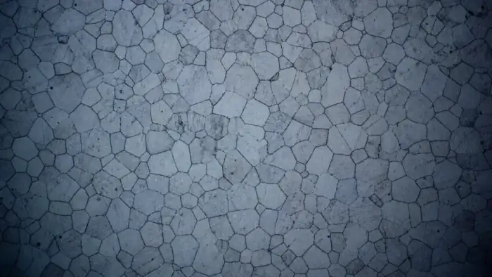
Grain size analysis
Average grain size and full distributions, traced automatically from etched micrographs.
MicrostructurePhase & microstructure fraction
Segment phases and constituents to quantify area fraction and spatial distribution.
 MicrostructureASTM E1245
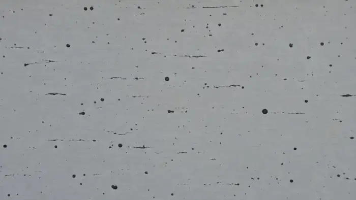
Inclusion & content rating
Detect and classify inclusions, then rate content by type and severity across fields.
 Microstructure
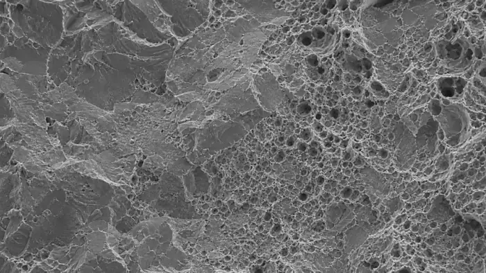
Fractography
Segment ductile dimple, cleavage, fatigue, and intergranular regions on fracture surfaces.
 Surface
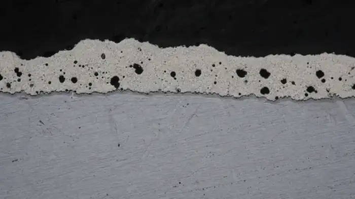
Coating thickness & porosity
Thickness profiles and sub-surface porosity from polished coating cross-sections.
 Surface
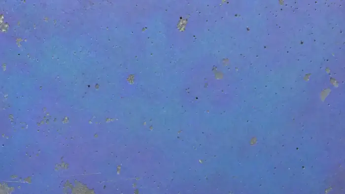
Coating & film coverage
Quantify surface coverage, holidays, and uniformity for films and thin coatings.
 Surface
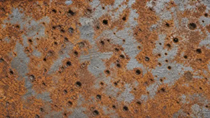
Corrosion & pitting
Segment rust by class, count pits, and track coverage across time points.
 Surface
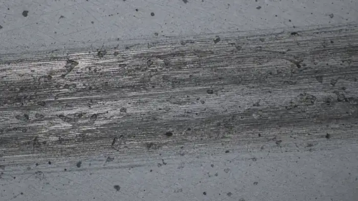
Wear, scratch & roughness
Measure wear tracks, scratches, and delamination from tribology and surface images.
 Surface
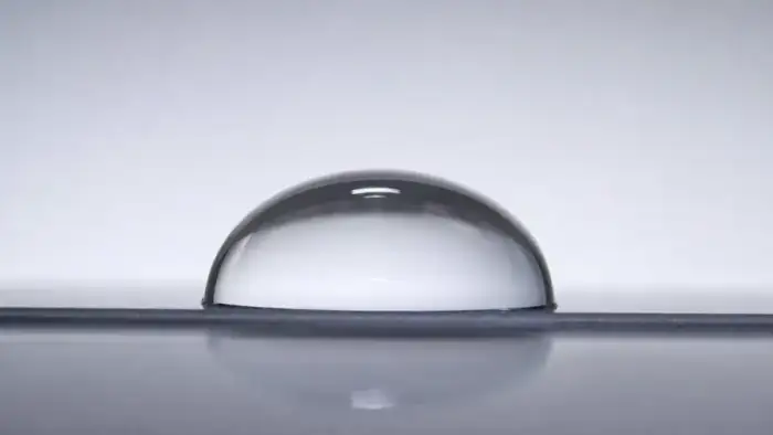
Contact angle & wettability
Extract droplet geometry and static contact angle from sessile-drop images.
 Surface
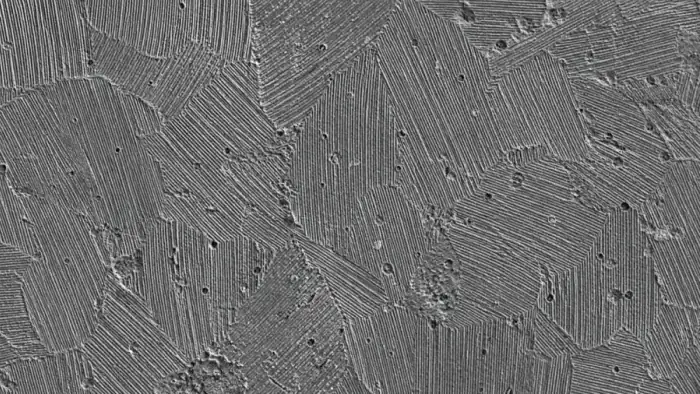
Surface texture analysis
Texture, domain size, and anomaly heatmaps from microscopy, SEM, and AFM exports.
 PowderISO 13322-1
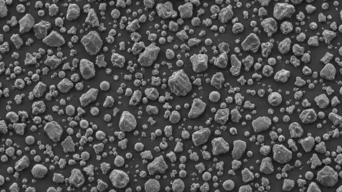
Particle size analysis
Static image-analysis particle sizing with shape descriptors across full fields.
 Powder
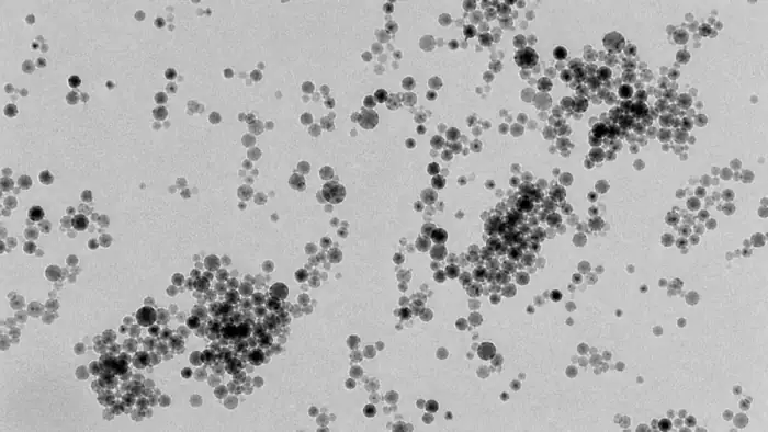
Nanoparticle analysis
TEM and SEM particle size, shape, and agglomeration for nanomaterials and catalysts.
 Powder
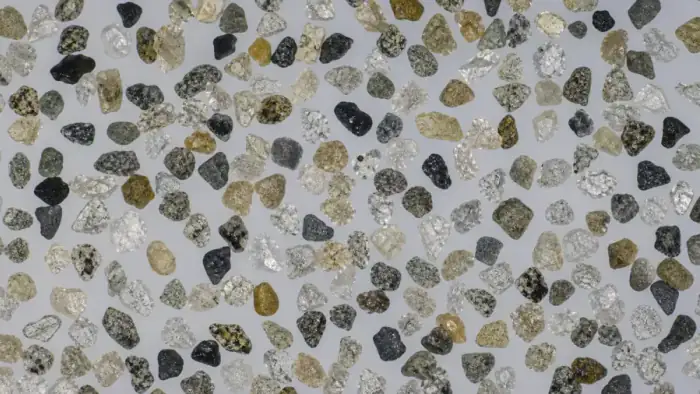
Mineral & granular analysis
Particle size, shape, and mineral-class proxies for mineral processing streams.
 TextileWorked example
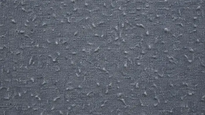
Textile pilling grade
Predict an ISO pilling grade from a fabric image, with density and the features behind the call.
 Textile
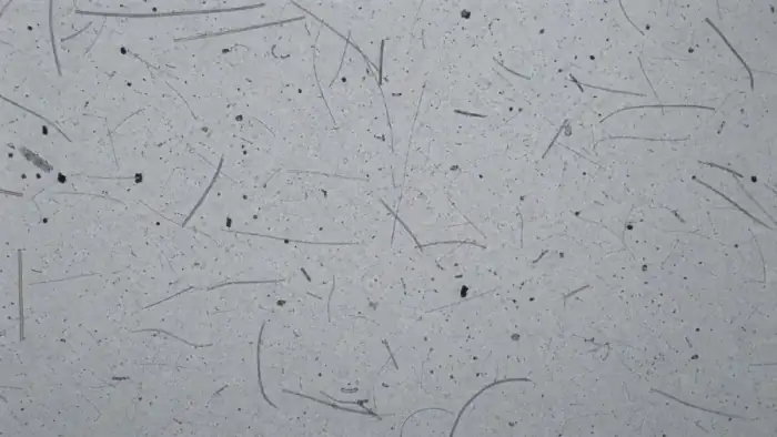
Fiber diameter distribution
Mean diameter, CV%, and D10/D50/D90 for wool, synthetic, and nanofiber, measured from the image.
TextileFabric inspection (4-point)
Detect fabric defects, assign demerit points by size, and total them per 100 square yards.
TextileCover factor & open area
Optical open area, pore size distribution, and cover uniformity measured on the actual fabric.
TextileForeign fiber contamination
Find polypropylene, coloured, and foreign fibers in the web before they reach the dyehouse.
TextileNep & trash count
Count neps, seed-coat fragments, and trash per gram of cotton web, sized and classified.
TextileDimensional stability & skew
Warp and weft shrinkage plus skew, measured from marked-square photographs before and after wash.
 Joining
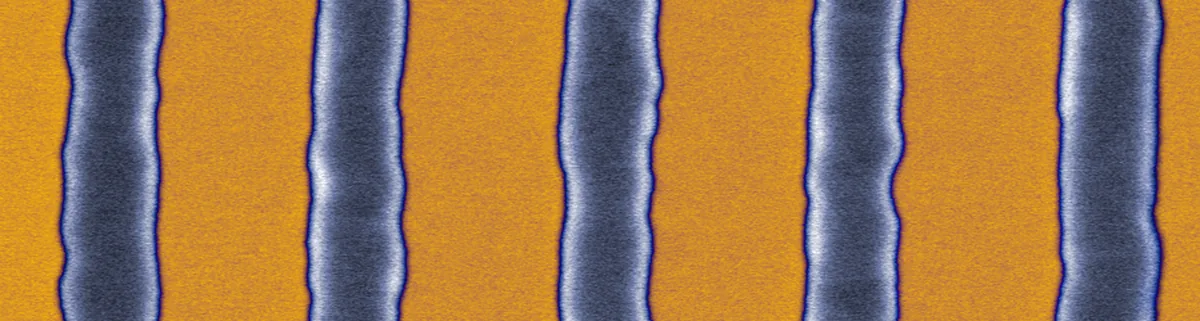
Critical dimension (CD) metrology
Line width, space, and via diameter measured from top-down images, with per-feature tables.
 Joining
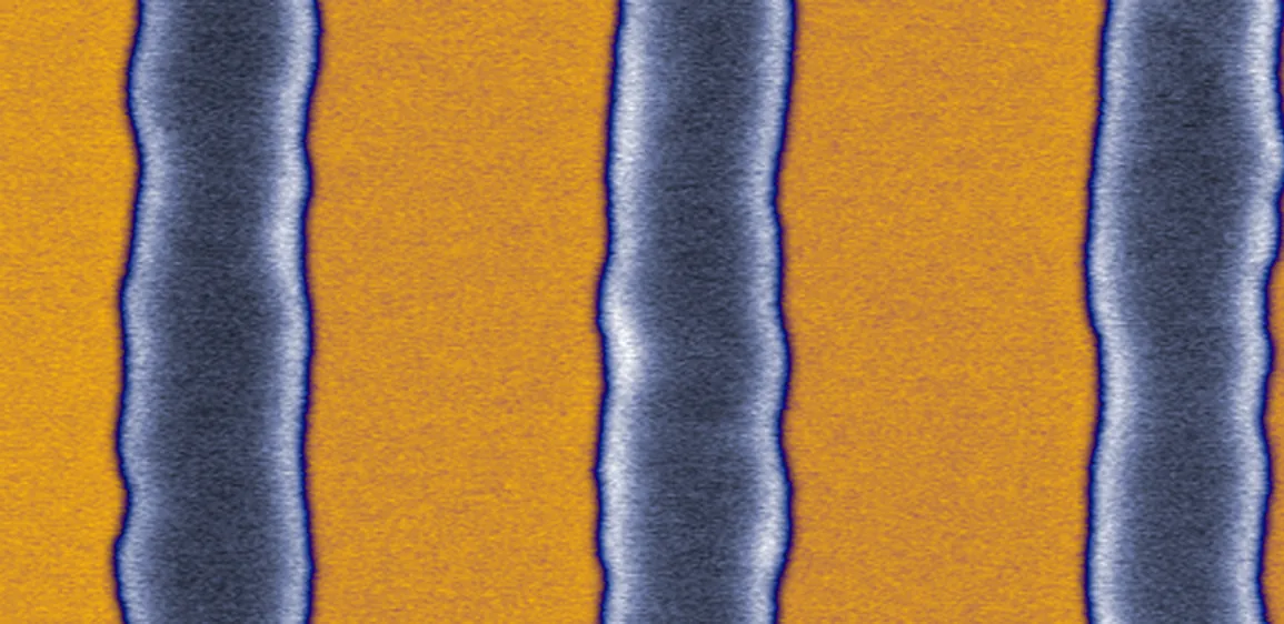
Line edge & width roughness (LER / LWR)
Line edge and line width roughness as 3-sigma deviation along patterned lines.
 Joining
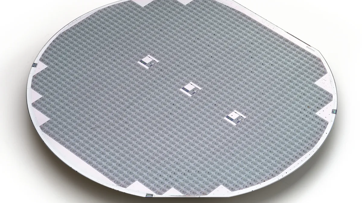
Wafer defect map & binning
Detect, locate, size, and bin defects across a wafer into a spatial map.
 Joining
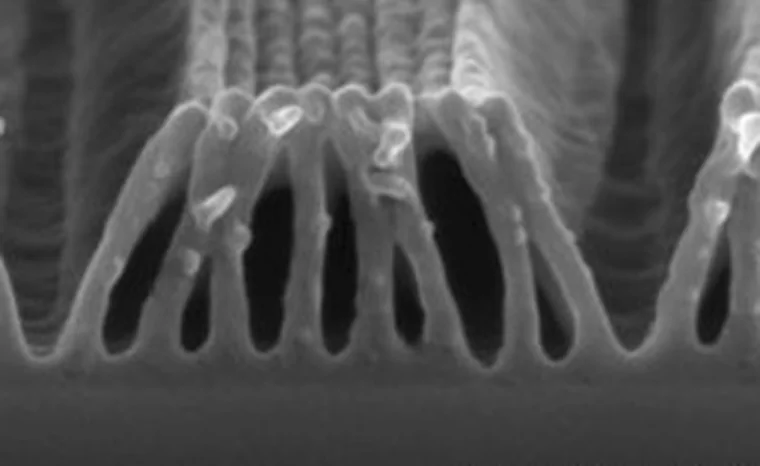
Photoresist pattern defects
Detect resist pattern collapse, bridging, footing, and scumming after develop.
 Additive
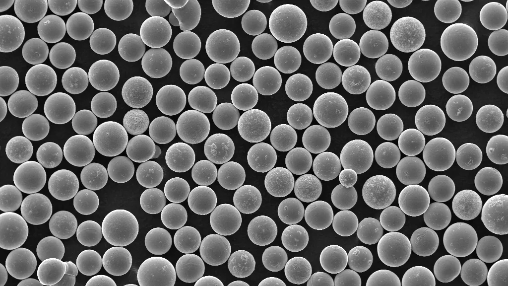
Metal powder feedstock QC
Particle size, sphericity, and satellite fraction for metal AM feedstock.
 Additive
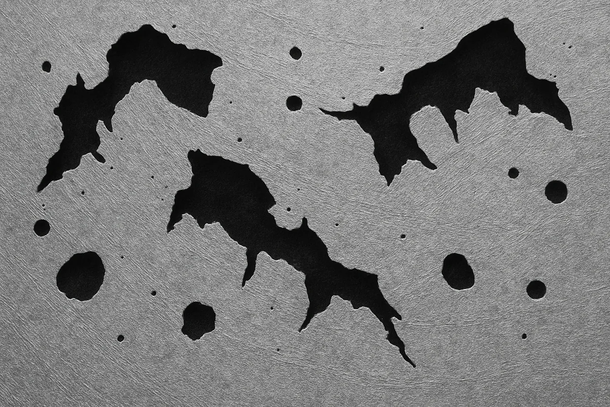
Printed-part porosity
Porosity fraction with lack-of-fusion versus gas-pore classification from a cross-section.
 Additive
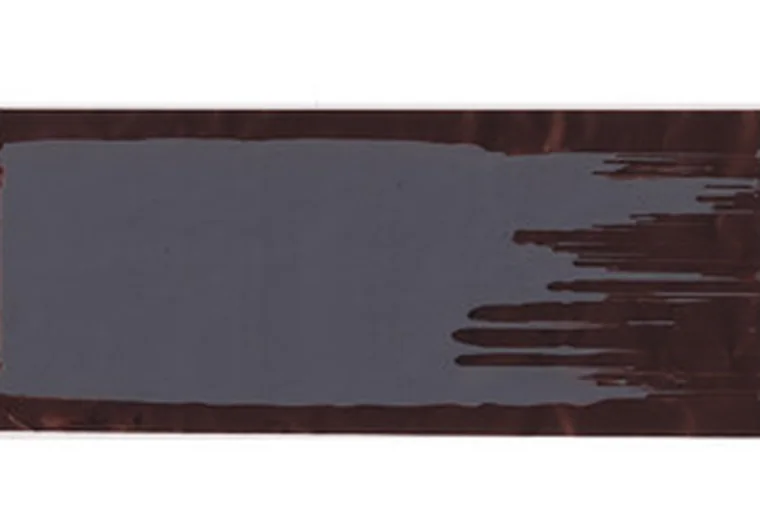
Battery electrode coating defects
Detect pinholes, agglomerates, streaks, and uncoated patches on electrode coatings.
 Joining
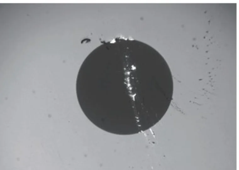
Fiber optic end-face inspection
Count and grade scratches and defects by zone on a connector end-face, per IEC 61300-3-35.
 Microstructure
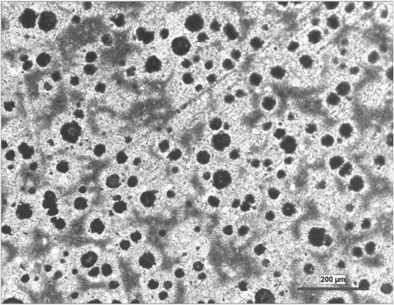
Graphite nodularity
Nodularity percentage and nodule count per mm2 for ductile and compacted graphite iron.
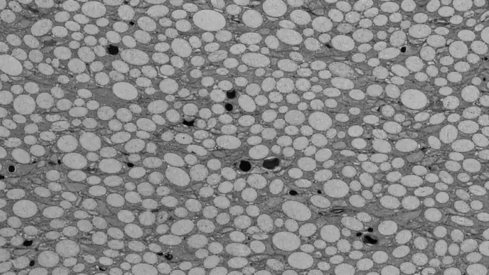 Textile
Composite fiber orientation
Fiber orientation, void content, and ply defects from polished sections and CT slices.
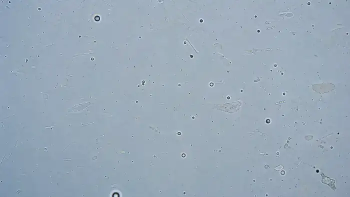
TextileFiber & inclusion analysis
Count and size fibers and inclusions, with area fraction and class breakdowns.
 Textile
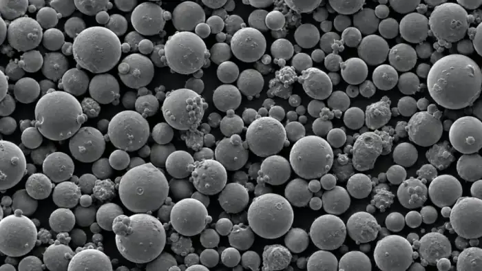
Polymer film & membrane defects
Pinholes, bubbles, scratches, and coverage uniformity for films and membranes.
 Additive
Additive manufacturing QC
From powder morphology to post-build cross-sections: layer anomalies and pore maps.
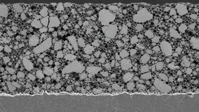 Additive
Battery electrode analysis
Coating, particle, pore, and crack measurements for electrodes, before and after cycling.
 Joining
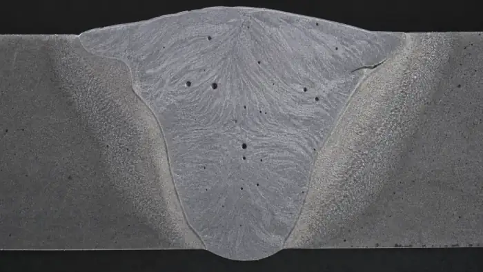
Weld defect analysis
Pores, cracks, fusion boundaries, and bead geometry from macro and microscopy.
 Joining
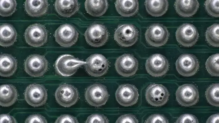
Solder joint inspection
Joint-quality classification and void measurement for solder and bond images.
 Joining
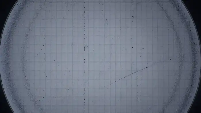
Semiconductor defect patterns
Classify wafer-map patterns and quantify defect clusters and densities.
 Joining
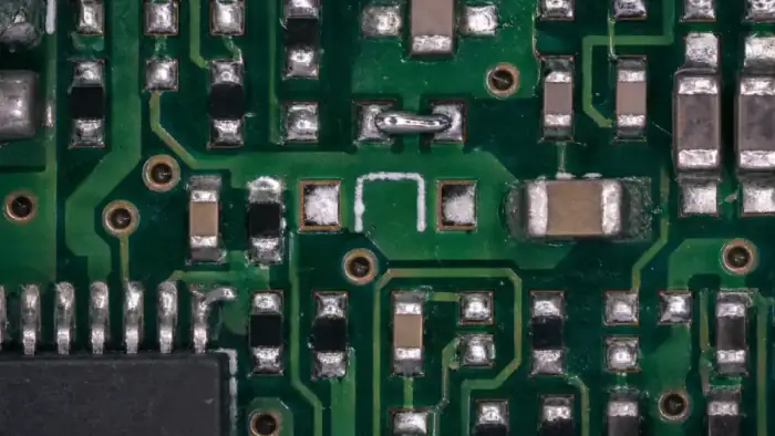
Electronics inspection
PCB and package inspection for missing, short, open, and contamination defects.
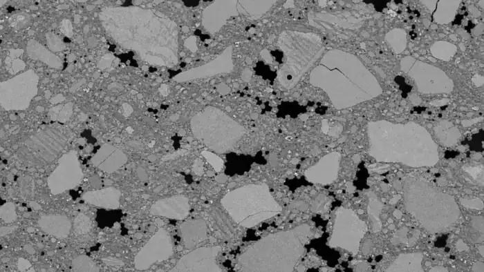 Geology
Digital rock & porosity
Pore fraction, throat proxies, and fracture density from micro-CT slices and SEM.
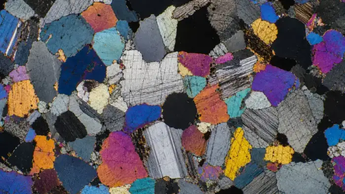 Geology
Petrographic thin section
Mineral phase maps, grain size, and sorting from thin-section microscopy.
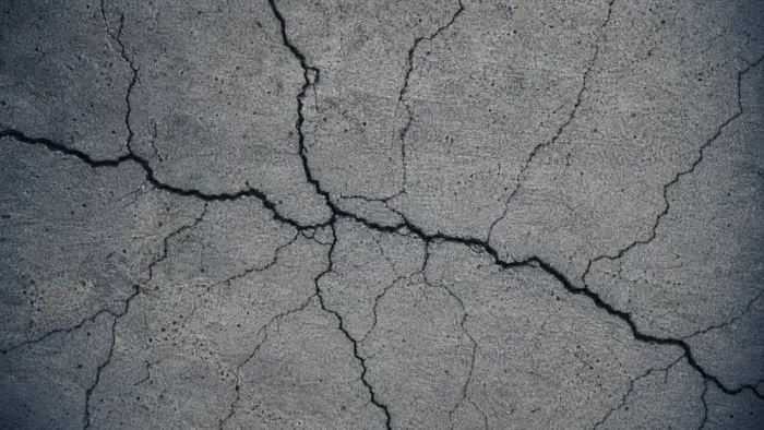 Geology
Crack detection & growth
Crack segmentation, length, width proxy, and growth over time for lab specimens.
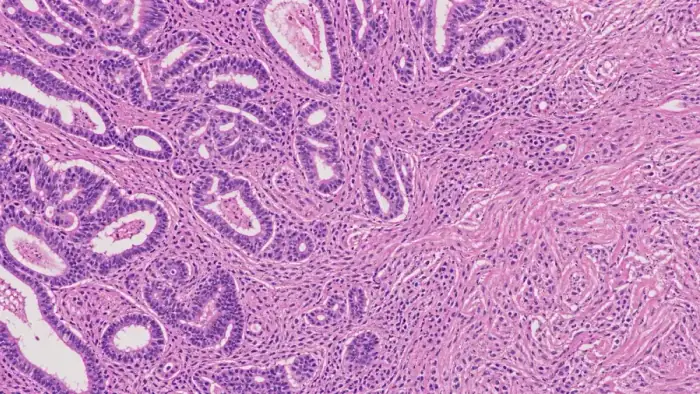 Adjacent life science
Pathology & histology
Region and feature quantification on stained tissue sections.
 Adjacent life science
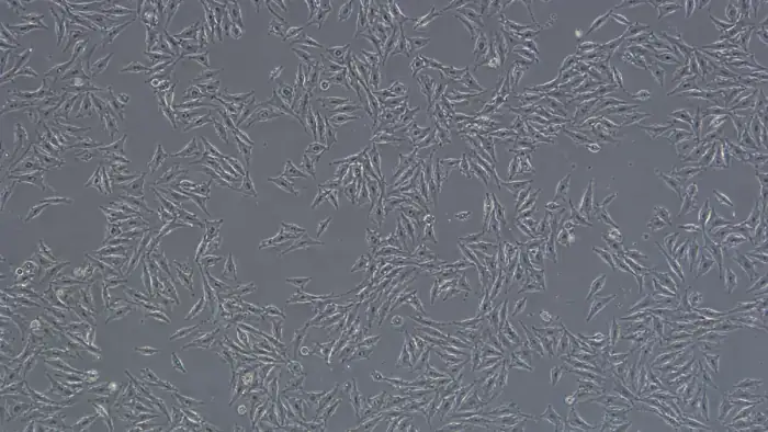
Cell counting & confluence
Counts, density, and confluence from brightfield and phase contrast.
 Adjacent life science
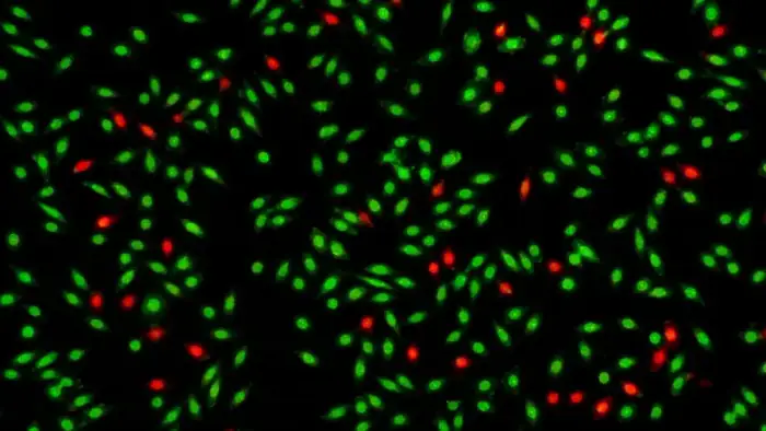
Viability & assays
Live and dead segmentation, viability ratios, and dose response.
Adjacent life scienceNuclear and RNA foci
Per-nucleus counts of intranuclear puncta: RNA foci, DNA-damage foci, FISH spots.
 Adjacent life science
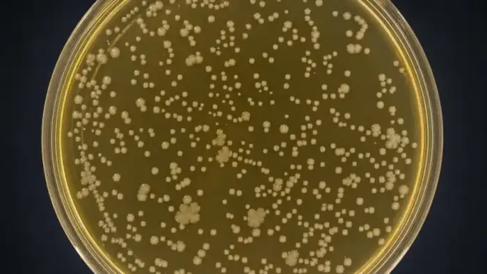
Colony counting
Automated colony counts across plates and dilution series.
 Adjacent life science
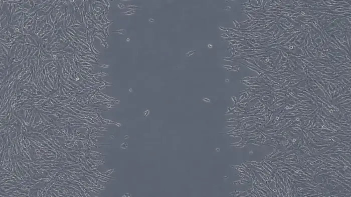
Scratch & wound assay
Wound area and closure over time from migration assays.
 Adjacent life science
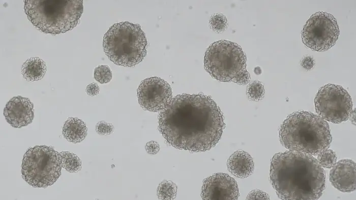
Organoid & spheroid
Size, count, and morphology of 3D culture structures.
 Adjacent life science
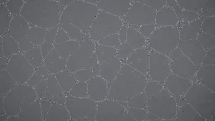
Angiogenesis & tubes
Network length, branch points, and node counts from tube-formation assays.
 Adjacent life science
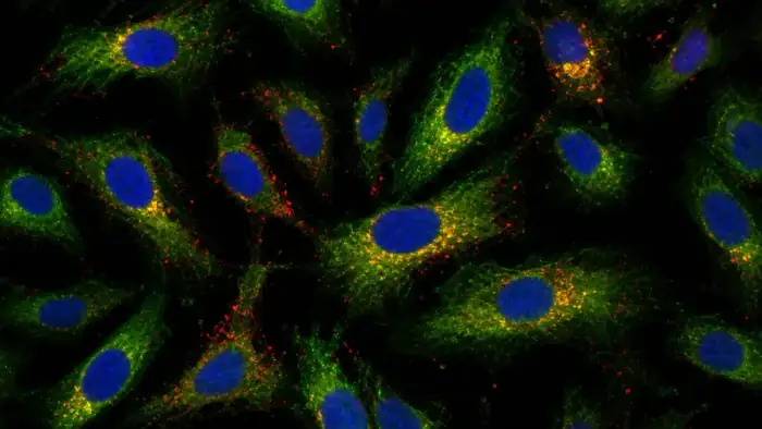
Fluorescence colocalization
Pearson, Manders, and Costes across multi-channel fields.
Built for standards-aware measurement, not black-box grading
ConductVision is designed to support the methods your lab already cites. We use careful claim wording: supported workflows, not certified compliance, until validated on your images.
| Workflow | Standard / method | ConductVision output | Claim wording |
|---|---|---|---|
| Grain size | ASTM E112, E1382 | Boundaries, intercepts, G-number, distribution | “Supports ASTM-style grain-size workflows” |
| Textile pilling | ISO 12945-2/-4, ASTM D4970 | Grade suggestion, density, heatmap, attribution | “Assists pilling assessment and QC review” |
| Particle sizing | ISO 13322-1 | Count, distribution, D10/D50/D90, shape | “Supports image-based particle sizing” |
| Inclusion rating | ASTM E1245, E45 | Inclusion count, area fraction, type, severity | “Supports inclusion quantification workflows” |
| Coatings | ASTM B487 | Thickness profile, coverage, bare areas, defects | “Measures thickness and coverage from calibrated images” |
| Porosity | Metallography / CT slice | Void fraction, pore size distribution, pore map | “Quantifies pore/void features from images” |
Worked exampleTextile pilling analysis for fabric R&D and QC
Upload fabric surface images, estimate an ISO-style pilling grade, review the regions that drove the call, and compare fiber, yarn, weave, and finishing parameters. ConductVision reports pill density, grade confidence, heatmap overlays, and SHAP explanations for production-factor review — the workflow where ConductVision already has unusually specific proof.
- ISO 1–5 grade suggestion
- Pilling density (pills/cm²)
- Grad-CAM heatmap overlay
- SHAP feature attribution
- Stage contributions: fiber, yarn, weave, finishing
- Batch comparison by lot, supplier, wash & abrasion cycle
Ten primitives behind every page
Every application is the same reusable engine, exposed under the name your field uses. Calibrate, detect, measure, review, export — then compare across lots and time points.
Scale calibration
Set real units from a bar or known dimension.
Object detection
Locate every object of interest in the field.
Semantic segmentation
Label each pixel by class: phase, pore, tissue.
Instance segmentation
Separate touching objects into countable instances.
Boundary tracing
Trace grain, cell, and region outlines precisely.
Crack & line detection
Follow cracks, fibers, and thin linear features.
Texture classification
Score surface texture, domains, and patterns.
Statistical export
Distributions and summaries, publication-ready.
Batch & lot comparison
Compare across cohorts, lots, and time points.
Overlay review
Inspect and adjust every result on the image.
The same image engine supports life-science assays
If the workflow is image in, measurement out, ConductVision can often support it with the same protocol, overlay, and export system — from histology to 3D culture.
Pathology & histology
Region and feature quantification on stained tissue sections.
Cell counting & confluence
Counts, density, and confluence from brightfield and phase contrast.
Viability & assays
Live and dead segmentation, viability ratios, and dose response.
Nuclear and RNA foci
Per-nucleus counts of intranuclear puncta: RNA foci, DNA-damage foci, FISH spots.
Colony counting
Automated colony counts across plates and dilution series.
Scratch & wound assay
Wound area and closure over time from migration assays.
Organoid & spheroid
Size, count, and morphology of 3D culture structures.
Angiogenesis & tubes
Network length, branch points, and node counts from tube-formation assays.
Fluorescence colocalization
Pearson, Manders, and Costes across multi-channel fields.
Validated on your image type, not a global accuracy number
Every high-stakes workflow needs validation on your samples. ConductVision supports locked protocols, reviewed overlays, and held-out validation sets so teams can document exactly how each measurement was produced — compared against expert manual measurements, held out by material family, supplier, microscope, and lighting, and labelled clearly when a protocol is still a custom or research workflow.
Send a sample image and a measurement goal
We will show the closest ConductVision workflow and identify what needs custom validation for your images.