Etch profile & high-aspect-ratio metrology
Measure trench width, depth, sidewall angle, bowing, taper, and bottom residue from cross-section images.
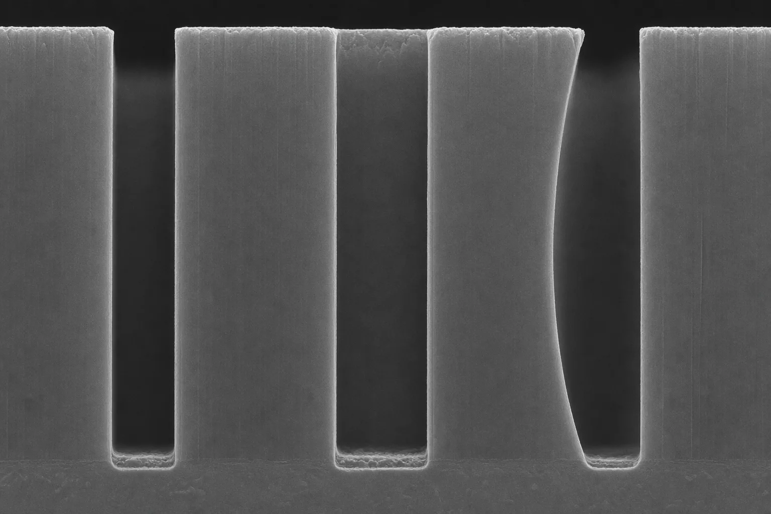
Example outputs shown for illustration. Numbers depend on your samples and protocol.
Image: Illustrative rendering (AI-generated, gpt-image-2), not an SEM image of a specific device
Results
Each measurement below comes from your own images, tied back to the annotated frame it came from, so results stay comparable across samples, locations, and conditions.
nm or µm
Trench width & depth
Perpendicular distance between the defined boundaries at each accepted measurement point.
Example, not a claimed result
In your report: Per-point values with median, spread, minimum, maximum, and location.
per area
Sidewall angle
Findings placed in sample coordinates to reveal spatial patterns and local density.
Example, not a claimed result
In your report: Coordinate-referenced map, regional density, and representative images.
per area
Bowing / taper
Findings placed in sample coordinates to reveal spatial patterns and local density.
In your report: Coordinate-referenced map, regional density, and representative images.
per area
Bottom-residue proxy
Findings placed in sample coordinates to reveal spatial patterns and local density.
In your report: Coordinate-referenced map, regional density, and representative images.
per area
Per-feature table
Findings placed in sample coordinates to reveal spatial patterns and local density.
Example, not a claimed result
In your report: Coordinate-referenced map, regional density, and representative images.
Built around your image set
Use the calibrated images your team already collects, together with the locations you need to compare.
Each report includes
The artifacts your team receives, ready for review and archive.
Annotated image set
Original images with regions of interest, measurement points, masks, and finding overlays.
Measurement table
Location-indexed values, units, distributions, and QC flags in a structured export.
Method record
Calibration evidence, analysis settings, version history, and validation summary.
Confidence in every resultTraceable measurements, reviewed against your agreed reference method.
- Traceable scale
- The report records the image scale, calibration evidence, and a method-specific expanded measurement uncertainty. It does not use one product-wide accuracy number.
- Reference comparison
- The configured method is compared with your accepted reference method or reviewed annotations, and reports bias by measurement range and image condition.
- Detection performance
- Detections are evaluated against reviewed reference regions with precision, recall, and segmentation overlap, separated by the conditions that affect performance.
- Repeatability
- The locked protocol is rerun on the same inputs and on a defined repeat set. The review records variation from image acquisition, sampling, and analysis separately where possible.
What this result does not establish: Measures geometry from prepared cross-section images. Cross-section preparation, image scale, charging, and site measurement rules determine absolute accuracy.
The measurement, today
High-aspect-ratio features are reviewed on a small number of manually annotated SEM cross-sections. Edge placement and the choice of measurement location can vary between analysts.
What it costs
A changing etch profile can alter downstream fill, resistance, or device behavior. Structured, image-linked measurements make profile differences visible across conditions.
From image to reviewed result
- 1
Acquire a cross-section
Load a prepared cross-section SEM, CD-SEM, or FIB-SEM image with a verified scale.
- 2
Identify the profile
Segment the feature sidewalls, opening, and bottom to establish the measurement geometry.
- 3
Measure each feature
Calculate configured width, depth, sidewall, taper, and residue measurements at consistent locations.
- 4
Compare conditions
Export overlays and per-feature tables for recipe, wafer, or lot review.
Not sure this is the right measurement?
Send a representative image and your measurement goal. A ConductVision scientist will confirm whether this is the right fit, or point you to the closer workflow, before you commit to a quote.
Related applications
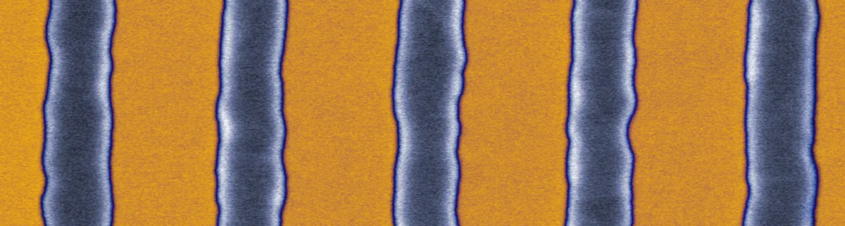
Critical dimension (CD) metrology
Line width, space, and via diameter measured from top-down images, with per-feature tables.
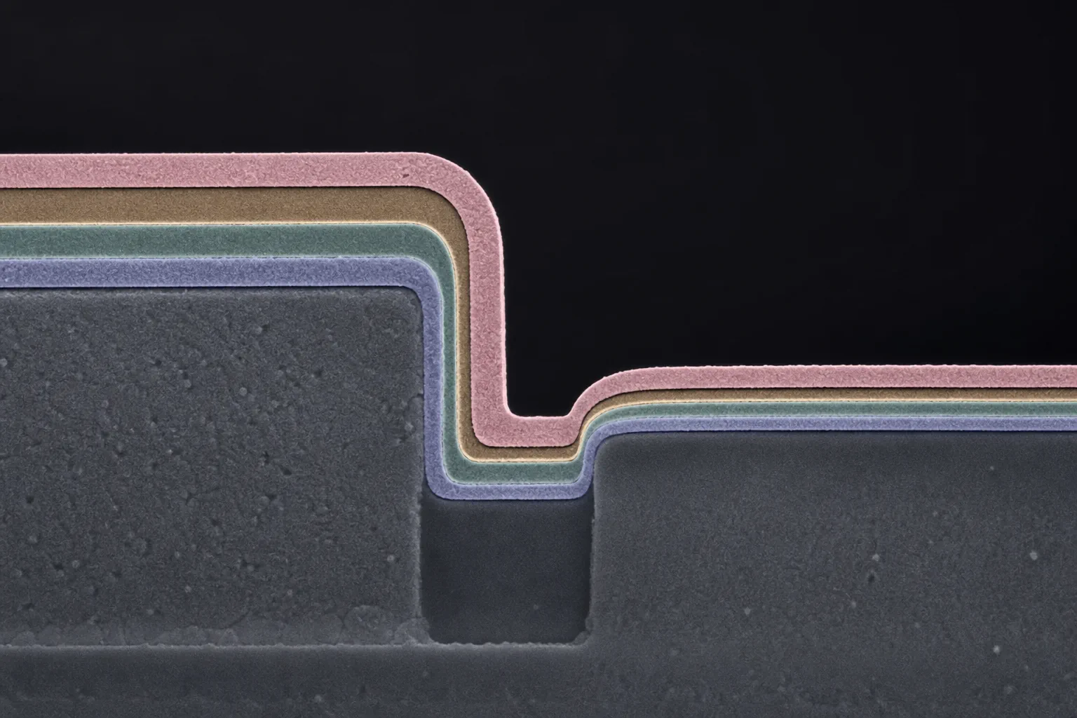
Thin-film step coverage & uniformity
Quantify layer thickness and step coverage across planar and topographic semiconductor features.
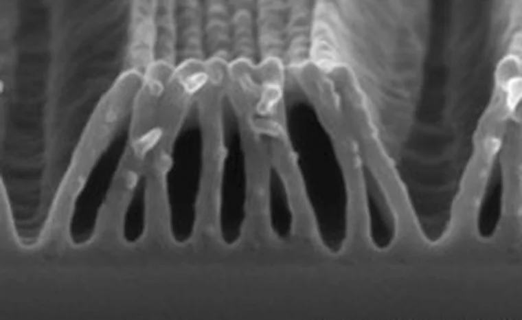
Photoresist pattern defects
Detect resist pattern collapse, bridging, footing, and scumming after develop.
Send a sample image and a measurement goal
We will show the closest ConductVision workflow and flag what needs custom validation for your images.