Thin-film step coverage & uniformity
Quantify layer thickness and step coverage across planar and topographic semiconductor features.
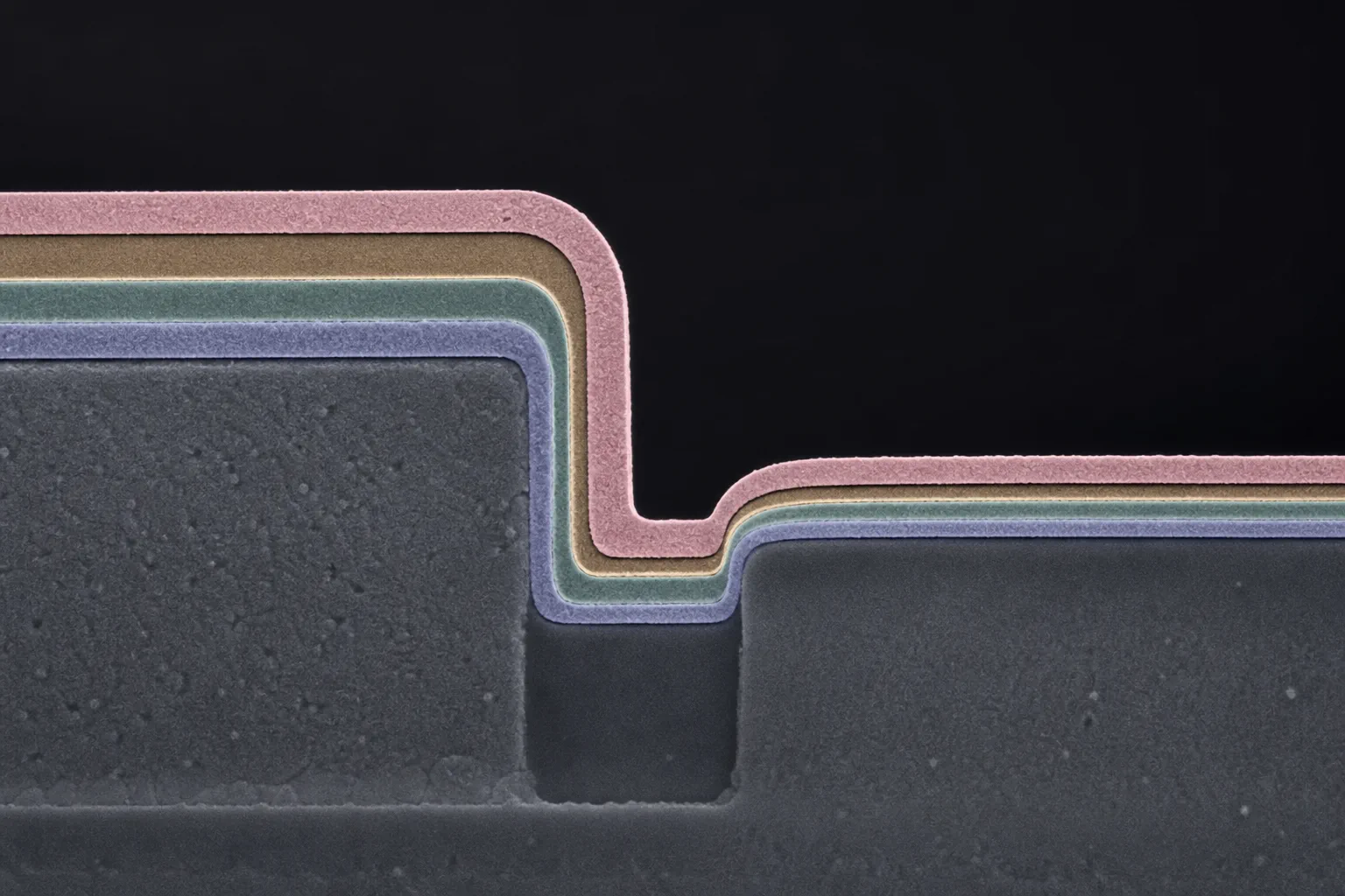
Example outputs shown for illustration. Numbers depend on your samples and protocol.
Image: Illustrative rendering (AI-generated, gpt-image-2), not a cross-section of a specific device
Results
Compare conformality and local thinning across a defined wafer, device, or coupon sampling plan before process-development review.
nm or µm
Local layer thickness
Perpendicular distance between the defined layer interfaces at each accepted sampling point.
Example, not a claimed result
In your report: Per-point table, median, P5/P95, minimum, maximum, and location identifier.
%
Step coverage
Local thickness at the sidewall or feature bottom divided by the agreed reference thickness on the field, multiplied by 100.
Example, not a claimed result
In your report: Per-feature coverage, distribution, and annotated reference locations.
% area
Void area fraction
Segmented void area divided by the eligible coating or fill area in the two-dimensional cross-section.
Example, not a claimed result
In your report: Per-field value, void-size distribution, and mask overlay. This is not a three-dimensional void volume fraction.
% length
Interface continuity
Length of visible interface meeting the agreed continuity rule divided by the eligible interface length.
Example, not a claimed result
In your report: Continuity value, gap locations, and the rule version used to classify a gap.
Built around your image set
Use the calibrated images your team already collects, together with the locations you need to compare.
Each report includes
The artifacts your team receives, ready for review and archive.
Annotated image set
Original images with regions of interest, measurement points, masks, and finding overlays.
Measurement table
Location-indexed values, units, distributions, and QC flags in a structured export.
Method record
Calibration evidence, analysis settings, version history, and validation summary.
Confidence in every resultTraceable measurements, reviewed against your agreed reference method.
- Traceable scale
- The report records the image scale, calibration evidence, and the method-specific expanded measurement uncertainty. It does not use one product-wide accuracy number.
- Reference comparison
- The configured method is compared with the customer’s accepted reference method or reviewed annotations and reports bias by thickness range and image condition.
- Detection performance
- Void and gap findings are evaluated against reviewed reference regions with precision, recall, and segmentation overlap, separated by the conditions that affect performance.
- Repeatability
- The locked protocol is rerun on the same inputs and on a defined repeat set. The review records variation caused by image acquisition, sampling, and analysis separately where possible.
What this result does not establish: Measures visible layer boundaries in supplied images. Material identity, optical-model choices, and calibrated thickness acceptance remain with your metrology method.
The measurement, today
Film thickness is often reported as one number from a monitor wafer, while local coverage around steps, vias, and corners is inspected separately and qualitatively.
What it costs
Non-uniform coverage can affect isolation, barriers, contacts, and subsequent etch behavior. A spatial measurement set exposes where a stack departs from its intended geometry.
From image to reviewed result
- 1
Load the layer images
Provide calibrated cross-section or thickness-map images from the surfaces and topography under review.
- 2
Separate the stack
Trace each visible layer and the feature geometry beneath it.
- 3
Measure coverage
Compare local layer thickness at the top, sidewall, and bottom of configured features.
- 4
Export the profile
Review thickness distributions, minimum locations, and annotated cross-sections together.
Thin-film step coverage and uniformity measurement
Step coverage describes how conformally a deposited film follows the topography of a feature: how thickness at a sidewall or feature bottom compares with thickness on the open field. ConductVision measures it directly from cross-section SEM, optical microscopy, and ellipsometry map images, so conformality, local thinning, and film thickness uniformity are quantified per location instead of inferred from a single monitor-wafer number.
Each engagement returns per-location layer thickness, step coverage percentage, void area fraction, and interface continuity, with every value tied back to the annotated image it came from. Results are compared against your accepted reference method and reported with method-specific measurement uncertainty, not a product-wide accuracy claim.
Common questions this answers
- Is the film conformal around vias, trenches, and corners?
- Where is the film thinnest, and by how much?
- How does step coverage compare across recipes, wafers, or lots?
- Are there voids or interface gaps in the deposited stack?
Related measurements: etch profile metrology, CMP scratch and planarization inspection, coating thickness and porosity.
Not sure this is the right measurement?
Send a representative image and your measurement goal. A ConductVision scientist will confirm whether this is the right fit, or point you to the closer workflow, before you commit to a quote.
Related applications
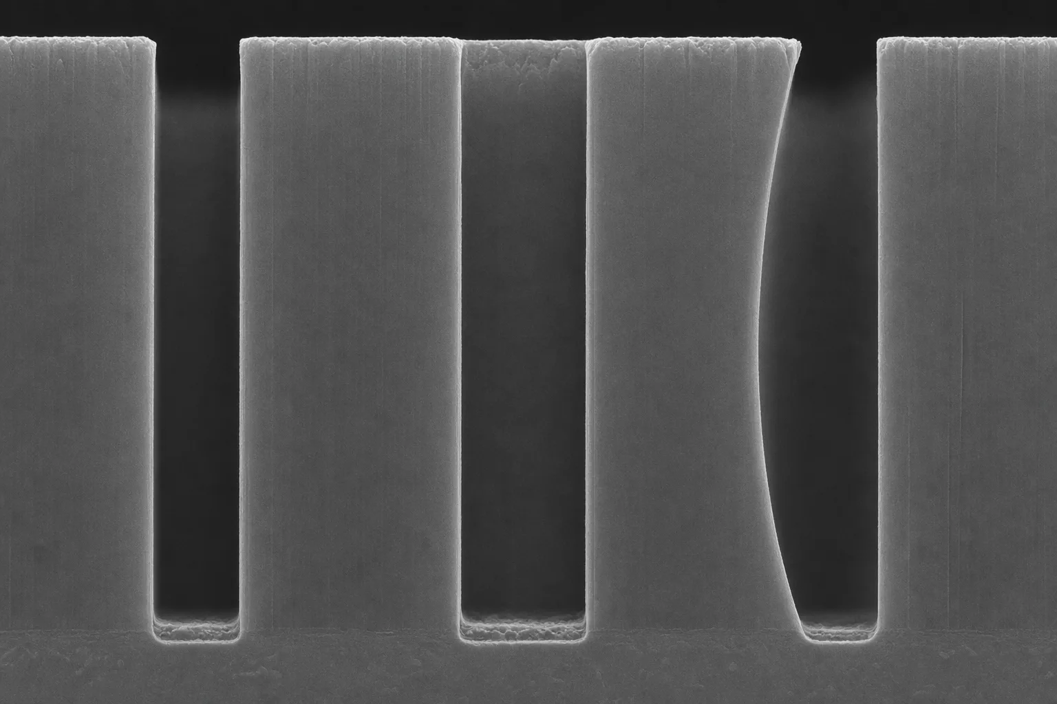
Etch profile & high-aspect-ratio metrology
Measure trench width, depth, sidewall angle, bowing, taper, and bottom residue from cross-section images.
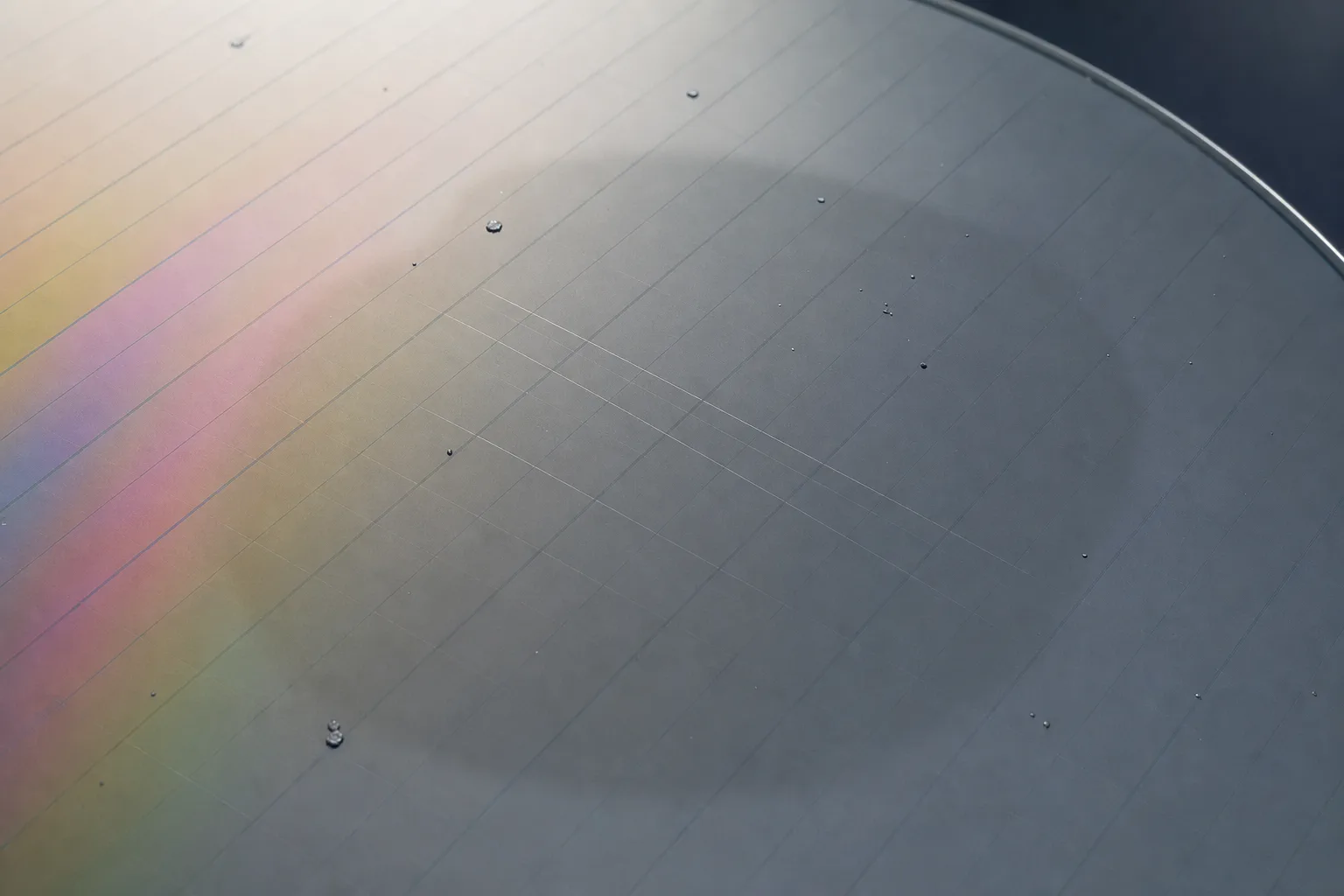
CMP scratch & planarization inspection
Locate scratches, residual particles, dishing, and erosion signatures after chemical mechanical planarization.
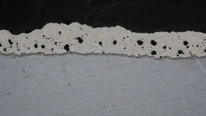
Coating thickness & porosity
Thickness profiles and sub-surface porosity from polished coating cross-sections.
Send a sample image and a measurement goal
We will show the closest ConductVision workflow and flag what needs custom validation for your images.