Reticle & photomask defect review
Locate missing features, pinholes, particles, and pattern deviations in reticle and photomask images.
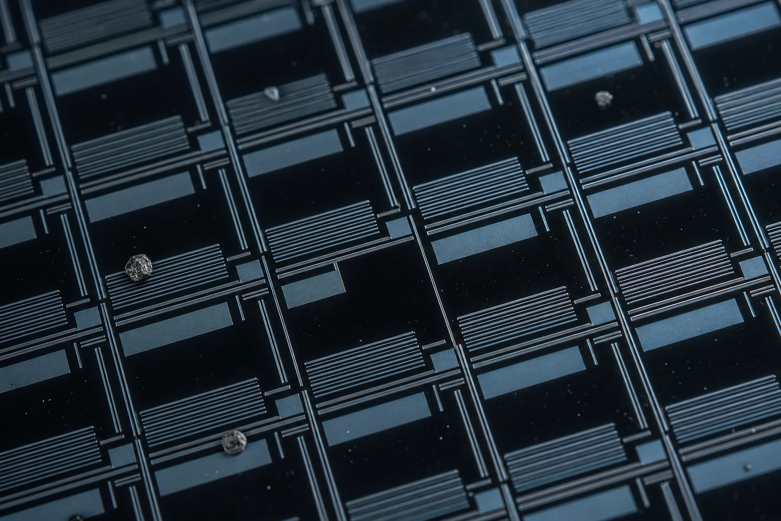
Example outputs shown for illustration. Numbers depend on your samples and protocol.
Image: Illustrative rendering (AI-generated, gpt-image-2), not an inspection image of a specific mask
Results
Each measurement below comes from your own images, tied back to the annotated frame it came from, so results stay comparable across samples, locations, and conditions.
per area
Defect location
Findings placed in sample coordinates to reveal spatial patterns and local density.
In your report: Coordinate-referenced map, regional density, and representative images.
class
Pattern-deviation class
Each detected feature assigned to a class using the agreed rule set, shown on the image.
In your report: Per-feature class, counts by class, and annotated overlays.
µm or count
Particle / pinhole count
Size and shape measured for every detected object, then summarized across the population.
Example, not a claimed result
In your report: Per-object table, size distribution, and summary percentiles.
µm or count
Size distribution
Size and shape measured for every detected object, then summarized across the population.
In your report: Per-object table, size distribution, and summary percentiles.
Built around your image set
Use the calibrated images your team already collects, together with the locations you need to compare.
Each report includes
The artifacts your team receives, ready for review and archive.
Annotated image set
Original images with regions of interest, measurement points, masks, and finding overlays.
Measurement table
Location-indexed values, units, distributions, and QC flags in a structured export.
Method record
Calibration evidence, analysis settings, version history, and validation summary.
Confidence in every resultTraceable measurements, reviewed against your agreed reference method.
- Traceable scale
- The report records the image scale, calibration evidence, and a method-specific expanded measurement uncertainty. It does not use one product-wide accuracy number.
- Reference comparison
- The configured method is compared with your accepted reference method or reviewed annotations, and reports bias by measurement range and image condition.
- Detection performance
- Detections are evaluated against reviewed reference regions with precision, recall, and segmentation overlap, separated by the conditions that affect performance.
- Repeatability
- The locked protocol is rerun on the same inputs and on a defined repeat set. The review records variation from image acquisition, sampling, and analysis separately where possible.
What this result does not establish: Supports image-based defect review. Mask disposition, printability, and any repair decision require the qualified inspection and lithography process used by your organization.
The measurement, today
Mask defects are often reviewed against reference imagery by hand. A finding may be obvious in a field yet difficult to quantify, classify, and retain for later comparison.
What it costs
A reticle defect can print repeatedly across a wafer. Early image review helps teams separate candidates for engineering review from cosmetic or imaging artifacts.
From image to reviewed result
- 1
Load inspection fields
Provide brightfield, darkfield, or microscope images with the reference pattern or a known-good field.
- 2
Align the pattern
Register repeated structures so missing, extra, and displaced features can be localized.
- 3
Classify candidates
Separate pattern deviations, pinholes, opaque particles, and image artifacts for review.
- 4
Export review evidence
Deliver a location-indexed list with the original and annotated inspection fields.
Not sure this is the right measurement?
Send a representative image and your measurement goal. A ConductVision scientist will confirm whether this is the right fit, or point you to the closer workflow, before you commit to a quote.
Related applications
Photoresist pattern defects
Detect resist pattern collapse, bridging, footing, and scumming after develop.
Critical dimension (CD) metrology
Line width, space, and via diameter measured from top-down images, with per-feature tables.
Semiconductor defect patterns
Classify wafer-map patterns and quantify defect clusters and densities.
Send a sample image and a measurement goal
We will show the closest ConductVision workflow and flag what needs custom validation for your images.