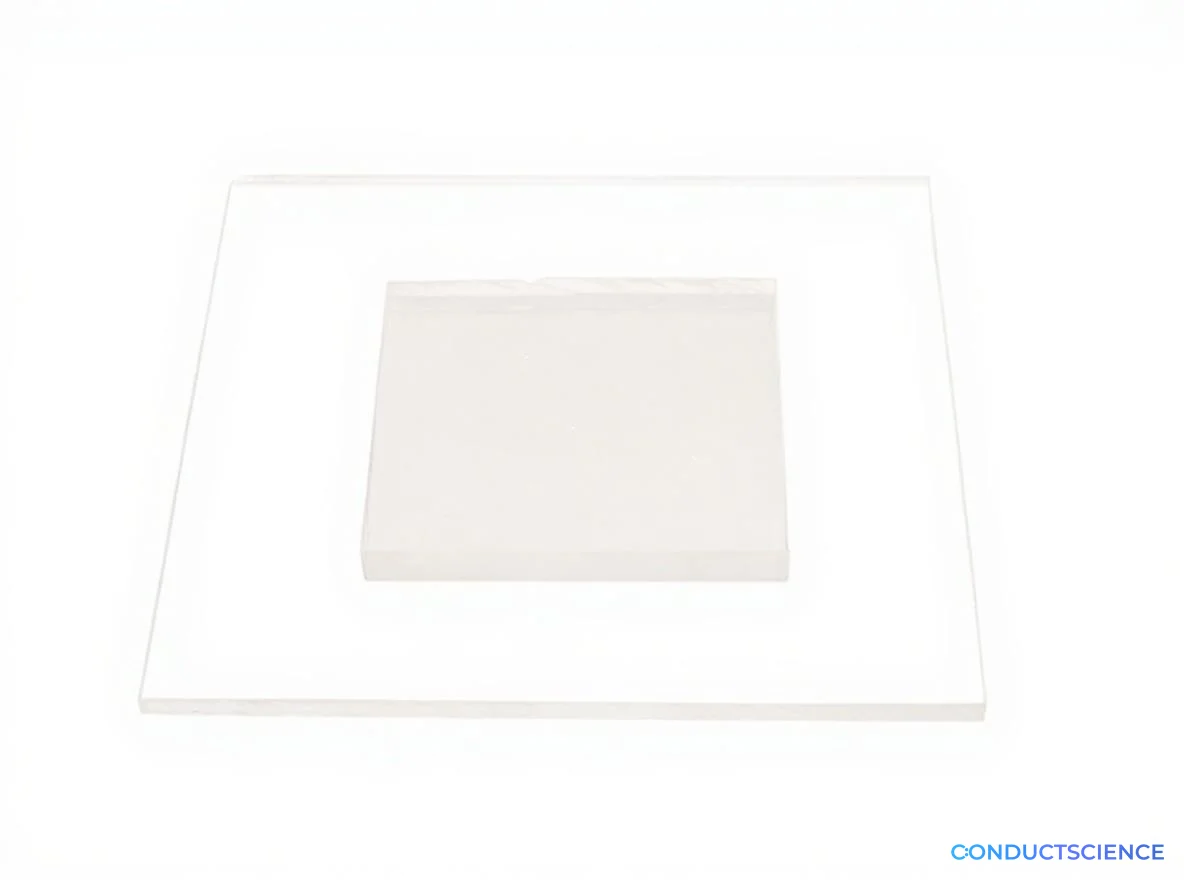
PMMA Board for Microfluidic Chips — 25-Pack
SKU PMMA-300-25PC-THICK
$2,500.00
$100.00/unit
IncludesStandard care
Optically transparent PMMA (acrylic) board for microfluidic chip fabrication.
>92% light transmittance, compatible with laser cutting, hot embossing, and solvent bonding. Available in thicknesses from 0.2 mm to 20 mm, multiple sheet sizes. Pack of 25.
Scientist guidance

Louise Corscadden, PhD
Director of Science · ConductScience
Ask Louise about PMMA Board for Microfluidic Chips — 25-Pack fit, setup, configuration, or quote prep.
Already working with us? Sign in to connect this with My Scientist.
Key Specifications
Full details →- Model fit
- 4 selectable configurations
- SKU family
- WHM-0171-25PK
- Shipping box
- 181.8 x 136.3 x 90.9 cm
- Ordering
- Online checkout and quote request available
- Category
- Lab Equipment
- Build notes
- Confirm accessories, station layout, and support needs before purchase
PMMA Board for Microfluidic Chips
High-quality polymethyl methacrylate (PMMA) boards designed for microfluidic chip applications and laboratory use.
Product Specifications
| Specification | Value |
|---|---|
| Board Size | 300 x 300 mm |
| Material | PMMA (Acrylic) |
| Thickness Options | 4 mm or less, or greater than 4 mm |
| Package Sizes | 10 pcs or 25 pcs |
| Pricing per Board | 4mm or less: $50 | Greater than 4mm: $100 |
Available Options
- 10 pcs / 4mm or less: $500 (10 boards x $50)
- 10 pcs / Greater than 4mm: $1000 (10 boards x $100)
- 25 pcs / 4mm or less: $1250 (25 boards x $50)
- 25 pcs / Greater than 4mm: $2500 (25 boards x $100)
Applications
- Microfluidic chip fabrication
- Lab-on-a-chip devices
- Microelectronics applications
- Laboratory prototyping
Frequently Asked Questions
- Q: What PMMA board thicknesses are available?
- A: PMMA boards are available in thicknesses from 0.2 mm to 20 mm. For boards under 4 mm thick, 300 × 300 mm pieces are available.
- Q: Can I order packs of 10 instead of 25?
- A: Yes. PMMA boards are available in packs of 10 or 25, depending on availability.
- Q: Can I mix different thicknesses in the same pack?
- A: No. Different thicknesses are quoted and supplied as separate packs.
- Q: Do the PMMA boards come with laser masking film or paper masking?
- A: No. The PMMA boards are supplied without laser masking film or paper masking.
Specifications
| Parameter | Value |
|---|---|
| Material | Polymethyl methacrylate (PMMA / acrylic) |
| Light transmittance | >92% (visible spectrum) |
| Available thicknesses | 0.2 mm, 0.5 mm, 1.0 mm, 2.0 mm, 3.0 mm, 5.0 mm, 6.0 mm, 8.0 mm, 10.0 mm, 12.0 mm, 15.0 mm, 20.0 mm |
| Standard sheet sizes | 100×100 mm, 200×200 mm, 300×300 mm, 400×400 mm, 600×600 mm; custom sizes available |
| Color options | Transparent (colorless), black opaque |
| Surface finish | Polished both sides |
| Chemical resistance | Resistant to dilute acids, bases, alcohols, and oils |
| Operating temperature | Up to 70°C continuous; up to 90°C short-term |
| Refractive index | ~1.49 at 589 nm |
| Pack size | 25 sheets per pack |
Key Features
- Exceptional optical clarity: Over 92% light transmittance enables fluorescence microscopy, brightfield imaging, and colorimetric detection directly through the chip substrate
- Machinability: Compatible with CO₂ laser cutting, CNC milling, hot embossing, and solvent bonding — supports full rapid prototyping workflows
- Broad thickness range: From 0.2 mm ultra-thin to 20 mm structural — accommodates master molds, channel layers, and cover plates in a single material system
- Chemical stability: Inert to common aqueous buffers, alcohols, and mild solvents; suitable for biological and biochemical assays
- Solvent bonding: Bonds readily with dichloromethane (DCM) or chloroform for chip assembly without specialized equipment
- UV transparency: Transmits down to ~300 nm, enabling UV detection and photopolymerization applications
- Consistent flatness: Polished both sides for uniform bonding contact and leak-free chip sealing
Applications
- Microfluidic chip substrates and cover plates
- Hot embossing master mold fabrication
- Droplet generation and digital microfluidics
- Cell culture chambers and organ-on-a-chip devices
- Point-of-care diagnostic chip prototyping
- Fluorescence and optical detection platforms
- Electrophoresis and DNA separation chips
- Lab-on-a-chip rapid prototyping
| Model | SKU | Listed price | Status | Shipping box |
|---|---|---|---|---|
| 25 pcs thick | PMMA-300-25PC-THICK | $2,500.00 | Available | 181.8 x 136.3 x 90.9 cm |
| 25 pcs 4 mm | PMMA-300-25PC-4MM | $1,250.00 | Available | 181.8 x 136.3 x 90.9 cm |
| 10 pcs thick | PMMA-300-10PC-THICK | $1,000.00 | Available | 181.8 x 136.3 x 90.9 cm |
| 10 pcs 4 mm | PMMA-300-10PC-4MM | $500.00 | Available | 181.8 x 136.3 x 90.9 cm |
No Q&A yet. Have a question? Ask below.
Have a question about this product?
Ask a question
Have a question? Just ask.
Send it over and we'll email you a personalized answer — no call, no scheduling.
Personalized email reply
Usually within one business day
Helpful answers published here
Prefer to talk it through?


PMMA Board for Microfluidic Chips — 25-Pack
$2,500.00
Added to quoteView Quote