ConductVision Enterprise

Electronics

Inspect microscale components at production speed with vision systems engineered for electronics precision.

Electronics operations

Electronics manufacturing demands inspection accuracy at the micron level across components that are too small and too numerous for reliable human evaluation. Solder joint quality, component placement accuracy, wire bond integrity, and surface mount defects must be verified at speeds that match automated assembly equipment. ConductVision's technology can provide high-resolution visual inspection models trained specifically for electronics manufacturing environments, including PCB assembly, semiconductor packaging, and final product verification. Cleanroom monitoring and ESD compliance tracking can provide additional operational oversight for sensitive production environments.

The challenge

Surface mount components are shrinking to 01005 packages (0.4 x 0.2 mm) that are invisible to unaided human inspection. Solder defects like cold joints, bridging, and insufficient wetting have distinct visual signatures but occur across thousands of joints per board. False reject rates from rule-based AOI systems waste significant operator time on phantom defects.

Our approach

ConductVision can deploy deep learning inspection models that achieve higher defect detection rates with significantly lower false reject rates compared to traditional AOI rule sets. Models can adapt to new component types through transfer learning, reducing new product introduction inspection setup from weeks to days.

Use cases

Solder Joint Inspection

High-magnification cameras can evaluate solder joint quality on SMT and through-hole assemblies, detecting cold joints, bridging, tombstoning, and insufficient wetting. Deep learning models can distinguish true defects from acceptable process variation, reducing false rejects.

Component Placement Verification

Post-placement cameras can verify component presence, correct orientation, polarity markings, and positional accuracy against design data. Missing or misaligned components can be flagged before reflow, preventing costly post-reflow rework.

Wire Bond and Die Attach Inspection

Semiconductor packaging inspection can verify wire bond loop height, tail length, ball placement, and die attach void coverage. Defects can be classified and tracked to specific bonder heads or tool settings for process correction.

Cleanroom Monitoring

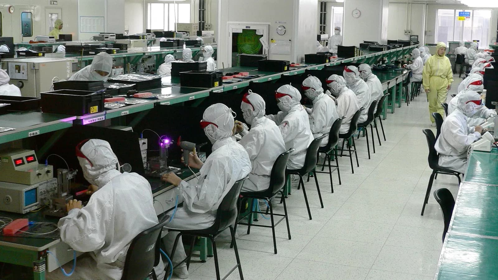
Cameras can monitor cleanroom gowning compliance, particle-generating activities, and door seal integrity. Personnel traffic patterns can be analyzed to identify contamination risk behaviors and optimize cleanroom layout and protocols.

ESD Compliance Tracking

Detection models can verify wrist strap usage, ESD smock wearing, and proper grounding practices at workstations. Compliance events can be logged for quality system auditing and correlated with field failure data for root-cause analysis.

Integration ecosystem

AOI Systems (Koh Young, CyberOptics)MES (Manufacturing Execution Systems)Pick-and-Place Machine ControllersSPC/Statistical Process Control PlatformsTraceability Systems (Aegis, Valor)

Scope a electronics monitoring pilot

Tell us about your sites and cameras; a ConductVision engineer replies with a scoping plan.