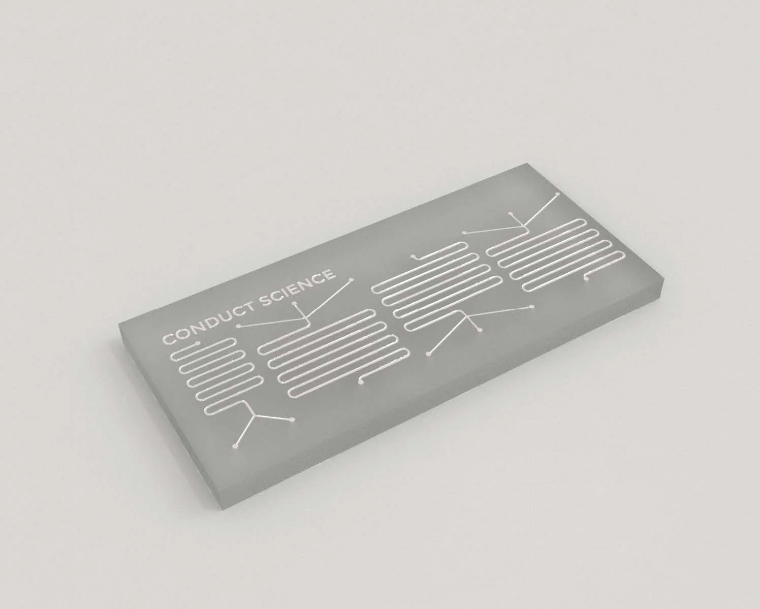
Microfluidic Chip Purchasing Guide for Biomedical Researchers

Learn More about our Services and how can we help you with your research!
- Introduction
- Key Factors
- Properties
- Treatments
- Compatibility
- Interfacing
- Comparison
- Recommendations
- Guidelines
- Conclusion
Introduction
Microfluidic chips are small devices—often only a few centimeters in size—that contain networks of tiny channels and chambers used to manipulate fluids at the microscale. In essence, a microfluidic chip miniaturizes laboratory processes (“lab-on-a-chip”), enabling the analysis and handling of very small sample volumes with high precision. These chips can integrate multiple steps of an experiment (such as sample preparation, mixing, reactions, and detection) into a single platform. By condensing what might require an entire bench of equipment into a palm-sized device, microfluidics offers faster processing, lower reagent consumption, and the ability to closely control experimental conditions. For example, microfluidic devices can mimic physiological flow conditions (like blood flow in capillaries) in vitro, which is invaluable for biomedical research.
Microfluidic chips have become increasingly significant in areas like diagnostics, drug development, and biomedical research. In point-of-care diagnostics, lab-on-a-chip technologies enable rapid, on-site tests for diseases and biomarkers. Everyday examples include home pregnancy tests and COVID-19 rapid tests, which use microfluidic principles to provide quick results. Such devices bring medical testing out of central labs and closer to patients, offering fast and often cost-effective diagnosis. In drug development, microfluidic chips allow high-throughput screening and complex cell culture models on a small scale. For instance, “organ-on-a-chip” systems can simulate human organ functions on a microfluidic platform, permitting more physiologically relevant drug toxicity and efficacy testing. These lab-on-a-chip devices are known for enabling rapid screening of drug candidates and can even be used to tailor personalized drug profiles, assessing efficacy and toxicity in vitro before clinical trials. More broadly, lab-on-a-chip technology is impacting fields like genomics, single-cell analysis, and environmental monitoring by providing compact, automated assays that were previously cumbersome. In summary, microfluidic chips are powerful tools that combine micro-scale engineering with biological and chemical experimentation, and their adoption in biomedical research is driven by the promise of doing more with less—smaller samples, faster results, and integrated workflows.
Explore our microfluidic chip for sale
Key Factors to Consider When Purchasing Microfluidic Chips
Choosing the right microfluidic chip for your application requires evaluating several technical factors. Especially for newcomers, it’s important to start with the basics and progressively consider more complex details. Below, we outline key factors – from materials and design features to connectivity and detection capabilities – that researchers should weigh before purchasing a microfluidic chip.
Material Choices
Why materials matter: The material from which a microfluidic chip is made fundamentally affects its performance and compatibility with your experiments. The ideal material often needs to balance multiple properties: optical clarity (for imaging or detection), chemical compatibility (with your samples and reagents), surface chemistry (to prevent unwanted molecule adsorption or to enable functionalization), and ease of microstructure fabrication. Common microfluidic chip materials include polymers (plastics), glass, and silicon, each with distinct advantages and disadvantages. Below we summarize popular material options:
-
PDMS (Polydimethylsiloxane): PDMS is a silicone elastomer and one of the most popular materials for microfluidic prototypes and academic research. Its popularity stems from its ease of fabrication and favorable properties. PDMS is optically transparent down to ultraviolet (UV) wavelengths, making it suitable for microscopy and fluorescence-based assays. It is also gas-permeable, which allows oxygen and CO₂ exchange – a critical feature for cell culture on-chip. Researchers can rapidly mold PDMS devices using soft lithography (pouring liquid PDMS over a micro-patterned mold and curing it), requiring only a simple mold and minimal equipment. This makes PDMS excellent for quick prototyping of new microfluidic designs. However, PDMS has notable drawbacks. It is hydrophobic by nature, which can lead to non-specific adsorption of small molecules and biomolecules. For example, PDMS tends to absorb hydrophobic drugs or dyes, potentially reducing the effective concentration of those molecules in your experiment. This absorption can skew results in drug screening or biochemical assays if not accounted for. PDMS also swells or degrades in the presence of many organic solvents, limiting its use to mostly aqueous (water-based) applications. Mechanically, PDMS is soft; high-pressure flows can deform channels, and tall narrow structures may collapse under its low elastic modulus. Additionally, while PDMS surfaces can be treated (e.g., by oxygen plasma) to become hydrophilic, these treatments are often temporary and the surface can revert to hydrophobic over time. In summary, PDMS is fantastic for early-stage research and cell culture applications due to its clarity, biocompatibility, and prototyping ease, but one must be cautious of its chemical incompatibilities and tendency to absorb or leach molecules.
-
Glass: Glass (often borosilicate glass or fused silica) is a traditional material for microfluidic chips, especially in analytical chemistry (e.g., capillary electrophoresis chips) and some commercial lab-on-chip devices. The biggest advantage of glass is its excellent chemical resistance and minimal background interference. Glass chips generally do not absorb small molecules or reagents, ensuring that concentrations of analytes remain stable – a stark contrast to PDMS absorption issues. Glass also has superb optical transparency across visible and UV wavelengths and very low autofluorescence, which means it won’t contribute unwanted background signal in fluorescence or optical detection assays. Surface chemistry of glass is well-understood; its silanol (Si–OH) groups can be readily modified using silane reagents, which is useful for covalently attaching biomolecules (like aptamers or antibodies) or creating defined surface coatings. Another benefit is that glass surfaces support stable electroosmotic flows, important for applications like electrophoresis. On the downside, glass chips are expensive and time-consuming to fabricate. Manufacturing typically involves cleanroom processes (photolithography and etching) and high-temperature bonding of glass wafers. This complexity means glass chips are usually made by specialized facilities or companies, not something a typical bio lab can prototype in-house easily. Glass is also a brittle material; chips can crack or break if mishandled. Additionally, glass (and silicon) chips are impermeable to gases, which is problematic for long-term cell culture on a chip – cells in a completely sealed glass device might suffer from limited oxygen unless the media flow provides sufficient gas exchange. In summary, glass microfluidic chips offer high chemical and optical performance ideal for analytical measurements, but at the cost of higher fabrication complexity and reduced gas permeability.
-
Thermoplastics (e.g., PMMA, PC, COC): Thermoplastic polymers are plastics that can be molded (often via injection molding or hot embossing) and are widely used for mass-produced microfluidic devices (such as disposable diagnostic cartridges). Common thermoplastics in microfluidics include PMMA (poly(methyl methacrylate), also known as acrylic or Plexiglas), PC (polycarbonate), and COC (cyclic olefin copolymer), among others. In general, thermoplastics are less expensive per chip when produced in large quantities and can be more robust than PDMS. However, each type has its own characteristics:
- PMMA: This plastic is highly transparent (up to ~92% transmission of visible light, even more than glass), making it suitable for optical detection and imaging. It is biocompatible and relatively easy to machine or mold. PMMA chips have been used in DNA separation, cell assays, and more. The drawbacks of PMMA are its limited chemical resistance and mechanical brittleness. PMMA can crack or craze under mechanical stress or with certain solvents, and it can be dissolved or damaged by many organic solvents. Thus, PMMA chips are typically confined to aqueous or mild chemical environments. Surface modification of PMMA (for example to attach biomolecules or change wettability) is possible, though not as straightforward as glass; treatments like UV/ozone or plasma can introduce polar groups on PMMA to reduce hydrophobicity.
- PC: Polycarbonate is another transparent thermoplastic often used when higher temperature or more durability is required. PC chips can withstand higher temperatures than PMMA (useful for applications like on-chip PCR thermal cycling). Polycarbonate is also less hydrophobic than some other plastics, which means aqueous fluids wet PC channels more easily. This can translate to more reliable filling of microchannels without air bubbles or the need for specialized surface coatings. However, a major limitation of PC for biomedical microfluidics is its autofluorescence. PC has an intrinsic fluorescence that can interfere with sensitive fluorescence-based assays. If you plan to do fluorescence imaging or detection, a PC chip may contribute background signal that lowers your signal-to-noise ratio. Additionally, like PMMA, PC is vulnerable to certain organic solvents (though it has better solvent resistance than PMMA in some cases) and may require surface treatment for certain applications.
- COC: Cyclic olefin copolymer is a newer polymer popular for microfluidic and biomedical devices. COC is highly transparent, including in the UV range, and exhibits very low autofluorescence, making it excellent for optical diagnostics (it’s often used in DNA analysis chips and optical microplates). It is also more chemically inert: COC has good resistance to polar organic solvents and very low water absorption, so it doesn’t swell or degrade easily in contact with fluids. COC is biocompatible and can be used for cell-based assays or clinical samples. One challenge with COC (and many thermoplastics) is that it is relatively hydrophobic, which can make it difficult to spontaneously fill microchannels with aqueous solutions (capillary flow) unless the surfaces are treated. Fortunately, there are established methods to modify plastic surfaces (e.g., plasma activation, coating with poly(vinyl alcohol) etc.) to make them more hydrophilic when needed. Overall, thermoplastic chips are a strong choice when you need a disposable, mass-producible device. They strike a balance between optical clarity and chemical compatibility, and different polymers can be chosen to suit the application (for instance, using solvent-resistant polypropylene or Teflon-like materials if organic solvents must be used). Keep in mind that obtaining thermoplastic chips often means either buying off-the-shelf devices or contracting a fabrication service, since making a high-quality thermoplastic microfluidic chip usually requires specialized equipment like injection molders or CNC micromilling machines.
In summary, material selection is a crucial first step when purchasing a microfluidic chip. If you are in early-stage research and need flexibility, PDMS-based chips might be ideal for their ease of use and biocompatibility, but be wary of their chemical limitations. For highly sensitive analytical applications or when solvent compatibility is paramount, glass or certain plastics like COC could be better. And for translating a proven design into a high-throughput or clinical setting, robust thermoplastics suitable for mass production will likely be the material of choice. Always consider the interaction of your sample/reagents with the chip material: factors like sample adsorption, solvent compatibility, and any required surface functionalization (discussed next) can often be traced back to material properties.
Channel Geometry and Surface Properties
The physical design of the microfluidic channels – their dimensions, shapes, and surface characteristics – plays a significant role in how experiments will run on the chip. Two key concepts for beginners to understand are laminar flow and surface wetting, as these are governed by channel geometry and surface properties:
-
Laminar vs. turbulent flow: In microfluidic channels, flows are typically laminar due to the small length scales and low Reynolds numbers. This means fluids move in smooth parallel layers with little to no mixing between streams unless deliberately engineered. As a result, mixing of reagents in a microchannel often relies on diffusion or special channel designs (like serpentine mixers or chaotic mixers) rather than turbulence. When evaluating a chip, consider the channel width, depth, and shape. Smaller channels (tens of micrometers) ensure laminar flow and can precisely control fluid contacts (useful for creating stable concentration gradients or interfaces), but they may mix slowly and can clog more easily. Larger channels (hundreds of micrometers) are more forgiving to clogging and can carry higher flow rates, but still remain laminar at typical microfluidic scales. If your application requires two different streams to mix, look for chips that include mixing structures or plan to implement methods like staggered herringbone ridges or droplet generators to enhance mixing despite laminar flow. Conversely, if you need to keep streams separate (as in some gradient generators or co-flow assays), a laminar regime is beneficial.
-
Channel geometry and cell/shear considerations: The cross-sectional shape of channels (e.g., rectangular vs. round) and the presence of features like pillars or chambers will impact cell-based experiments. For cell culture on chip, wider and shallower channel regions can serve as culture chambers, but the shear stress from flow needs to be appropriate for the cells. Long, straight channels are common for perfusion of cells or organs-on-chips, whereas zigzag or constricted channels might be used for cell sorting or filtration. If you plan on seeding cells inside channels, ensure the chip design includes provisions for that (such as connection ports that can be temporarily plugged, or chambers that accommodate cell loading). High-aspect-ratio channels (very tall relative to width) can sometimes collapse in softer materials (like PDMS), so check that the chip’s material and design are suitable for the structures it contains.
-
Surface wetting and capillary action: The surface properties (hydrophobic or hydrophilic) of channel walls determine how easily fluids can enter and move through the channels, especially under capillary forces. A hydrophilic surface will cause aqueous solutions to spread and wick into channels spontaneously, which is crucial for capillary-driven microfluidics (where no external pump is needed to draw fluid in). Hydrophobic surfaces, by contrast, can cause liquids to bead up and resist filling the channel. For example, many thermoplastic chips are somewhat hydrophobic and might require a priming step or surface treatment to fill smoothly. Some chip designs take advantage of surface properties: open microfluidic devices often rely on patterned hydrophilic pathways on an otherwise hydrophobic surface to guide droplets. In paper microfluidics (like lateral flow tests), the cellulose paper is hydrophilic and wicks fluid. In closed chips, if passive capillary flow is a feature (like in certain point-of-care devices where you just touch a drop of blood and it fills the network), those channels must be hydrophilic. On the other hand, for droplet microfluidics (water-in-oil droplets), channel surfaces are typically rendered hydrophobic so that the aqueous droplets don’t wet the walls and can be cleanly transported in an oil phase. Think about your assay’s wetting needs: Will you be pushing liquid by external force (then surface energy is less critical), or do you rely on capillary action? If the chip material is hydrophobic (e.g., PDMS or many plastics) and you need capillary flow, ensure the chip either comes pre-treated to be hydrophilic or be prepared to treat it yourself. Even within the same material category, surface treatments can make a difference: for instance, polycarbonate is naturally less hydrophobic than COC, giving it better initial filling behavior for water. Many manufacturers will specify if their chips are hydrophilized or not.
-
Surface roughness and coating: Microfabrication methods influence surface smoothness. For most biomedical applications, smooth channel walls are desirable (to prevent unwanted turbulence and reduce sites for particles/cells to get stuck). If a chip is fabricated by high-quality molding or etching, surfaces are usually smooth. 3D-printed channels, in contrast, might have layer lines or roughness that could affect flow or imaging. Additionally, some chips may have surface coatings (e.g., a PDMS chip coated with a thin glass-like layer, or a plastic chip coated with reagents). For example, microfluidic devices intended for electrophoresis often have coatings to control electroosmotic flow; chips for cell culture might be coated with extracellular matrix proteins to help cells adhere. When purchasing, check if the chip’s surfaces are untreated or treated, and if treated, whether the coating suits your needs (and if it’s stable under your conditions).
In summary, examine the design specs of candidate chips: channel dimensions, shapes, and any noted surface treatments. A well-designed chip for your application will have geometry that supports the fluid behavior you need (laminar flow, mixing, separation, etc.) and surface properties compatible with your assay (proper wetting, minimal non-specific binding). Don’t hesitate to reach out to manufacturers for details on surface properties if it’s not clear – for instance, whether you need to pretreat the chip to make it wettable. Remember that you can often adjust surface properties (with treatments discussed next), but the channel geometry is fixed once the chip is made, so it should be matched to your experimental requirements from the start.
Hydrophilization and Surface Treatments
Because surface chemistry is so important in microfluidics, many chips require surface treatment either during manufacturing or by the end-user to tailor the chip’s internal surfaces for a specific purpose. “Hydrophilization” refers to making a surface more hydrophilic (water-attracting). This is commonly done to promote fluid flow in microchannels and to reduce issues like air bubble entrapment. For example, native PDMS is hydrophobic and often needs to be treated by oxygen plasma to introduce –OH groups on its surface, making it temporarily hydrophilic. This plasma treatment helps liquids wet the channels uniformly and also enables bonding of PDMS to glass or another PDMS layer (plasma activates the surface so that two pieces can form a permanent seal). However, one should be aware that some treatments are not permanent. In the case of PDMS, the plasma-induced hydrophilicity “ages” – within minutes to hours, the surface can gradually return to its hydrophobic state as hydrophobic polymer chains migrate to the surface. If you purchase a plasma-treated PDMS chip, use it as soon as possible or inquire whether it has a protective storage method to preserve hydrophilicity. There are chemical coatings that can make PDMS surfaces hydrophilic more permanently (e.g., silanization with hydrophilic silanes, or grafting hydrophilic polymers), but these add complexity.
Aside from wetting, surface treatments are also used for functionalization – attaching biochemical moieties to the channel walls. This is crucial for chips that perform immobilization-based assays (such as ELISA-on-chip, DNA hybridization, or aptamer-based capture). A variety of methods exist: silane chemistry on glass (e.g., silanizing with an amine or epoxy-silane to then link biomolecules), polymer coatings on plastics, or using specialty surface chemistries provided by the manufacturer. Some microfluidic chips come pre-functionalized (for example, a chip with antibody-coated microchannels for capturing circulating tumor cells). Most, however, come as blank surfaces and it’s up to the researcher to functionalize if needed. Consider what you need to stick to the channel walls (if anything). If nothing (i.e., you want inert walls to prevent any binding), then materials like PDMS might actually be problematic because proteins and small molecules can adsorb to them by default. In such cases, you might implement surface blocking (with BSA, casein, or commercial blocking agents) or use a different material with low adsorption (like coated glass or a hydrophilic polymer coating). If you do need to attach something (like an aptamer or antibody), check that the material can be functionalized. Glass and silicon are very amenable to surface chemistry via silanol groups. Thermoplastics often require introducing functional groups onto their surface; for instance, polystyrene (common in cell culture and also used in some microfluidic devices) has a hydrophobic surface that can be made hydrophilic or functional via plasma, UV, or chemical treatments. Manufacturers sometimes offer chips with custom surface treatments if you ask.
Examples of common surface treatments:
- Plasma oxidation: Exposes the surface to an oxygen plasma, adding polar groups (good for hydrophilicity) and enabling bonding of parts. Often used on PDMS, thermoplastics, and polystyrene. The effect may wane over time, especially on PDMS.
- Silanization: Coating a glass or oxidized surface with organosilanes. For example, silanizing with (3-aminopropyl)triethoxysilane (APTES) adds amine groups to which one can link biomolecules. Silanes with PEG chains can make surfaces non-fouling. This is a versatile method for glass and silicon chips.
- Polymer coatings: Filling and incubating the channels with solutions that deposit a coating. Polyethylene glycol (PEG)-based coatings or polydopamine coatings can create bioinert surfaces. Some researchers coat PDMS channels with a thin PDMS-compatible polymer that prevents absorption of molecules (to mitigate PDMS’s tendency to soak up hydrophobic drugs.
- Surface grafting: Using UV or chemical initiators to graft monomers inside channels, creating a polymer brush lining. For instance, grafting polyacrylamide or poly(ethylene glycol) can resist protein adsorption.
- Specialty treatments: For certain applications, you might need unique surfaces (e.g., a chip for electrophoresis might have walls coated to suppress electroosmotic flow, or a chip for cell adhesion might be coated with collagen or fibronectin).
If you are buying a chip, find out if the chip is ready-to-use or requires surface prep. Some off-the-shelf chips for diagnostics come pre-treated (for example, hydrophilized and packaged in liquid to maintain the treatment). Others, especially generic PDMS chips, might arrive untreated and you’ll need to plasma-treat or coat them yourself. Ask the supplier for protocols if you’re unsure; they might have recommended treatments for their material.
Finally, it’s worth noting that ongoing innovations aim to create materials or coatings that eliminate some of these surface issues. Researchers have explored permanent hydrophilic PDMS variants, silicone formulations that resist absorption, and sol-gel coatings that line channels with glass-like layers. While these might not be standard in commercially available chips yet, being aware of the surface chemistry options will help you make the most of whatever chip you choose or to request custom modifications if necessary.
Compatibility with Sensors, Aptamers, and Biochemical Assays
Microfluidic chips often serve as more than just passive fluid conduits – they frequently incorporate sensors or are used in conjunction with biochemical assays that have specific requirements. When choosing a chip, consider how it will interface with detection methods and biological components:
-
Integration of sensors (electrical, optical, etc.): If your experiment involves measuring signals from within the chip, you’ll need compatibility between the chip and the sensor hardware. For instance, many lab-on-chip systems use optical detection (fluorescence, absorbance) by placing the chip under a microscope or a photodetector. In such cases, the chip’s material must be optically clear at the relevant wavelengths (see Optical properties below) and of appropriate thickness for the working distance of lenses. If the chip includes built-in optical components (like waveguides or lenses molded into the chip), ensure those are aligned with your instrument. For electrochemical sensing or electrical manipulation (e.g., electrodes for impedance sensing, electrophoresis, or DEP – dielectrophoresis), note that most microfluidic materials are insulators. Thus, chips that use electrodes typically have those electrodes fabricated from metals or conductive coatings integrated into the chip design. PDMS chips, for example, cannot have embedded metal electrodes easily due to the soft lithography process, so the common workaround is to fabricate electrodes on a glass substrate and bond the PDMS channels on top. If you need an electrode-integrated chip (say for sensing or electroporation), you might prefer glass or silicon-based chips where lithographed electrodes are available, or polymer chips that come with electrode patterns. Check if the vendor offers versions of the chip with electrodes or if you are expected to incorporate them (some researchers stick gold foil or wires into channels as a DIY solution, but that’s not very reproducible). In summary, match the chip to your detection mode: a chip for use with a microscope should be microscope-slide sized or have a transparent window for viewing; a chip for electrical readouts might need ports or flat areas to attach electrodes or PCBs.
-
Aptamers, antibodies, and surface-bound assays: Many biomedical microfluidic applications involve capturing target molecules (or cells) on a surface within the chip using affinity reagents like aptamers or antibodies. If you aim to perform such an assay, the chip’s surface chemistry must allow for immobilization of these capture molecules. Glass and silicon chips provide silanol groups for robust chemical attachment via silane reagents, which is ideal for creating a functionalized surface. Thermoplastics often require pretreatment (e.g., a carboxylate coating or an epoxy layer) to facilitate protein or DNA attachment. Some commercial chips (often those meant for immunoassays) might be sold with a pre-activated surface (for example, streptavidin-coated channels so you can introduce a biotinylated aptamer that will stick). If not, you will need to functionalize the surface yourself – consider whether you have the means to do that on the given material. PDMS, in its native form, is not very conducive to covalent immobilization of biomolecules, but techniques exist (e.g., plasma-treating PDMS and then silanizing with an amine-silane, or using a poly-L-lysine coating for electrostatic binding). Polycarbonate and polystyrene surfaces can be modified similar to standard ELISA plates (they can adsorb proteins via hydrophobic interactions or be treated to have COOH/NH₂ groups). The efficiency of aptamer or antibody immobilization, and the retention of their activity, can vary widely by material and treatment. If you find references or application notes of similar assays, they can guide what material is best. For example, one study demonstrated enhanced aptamer immobilization in microfluidic channels by using a dendrimer-based surface coating, which would be an important consideration if buying a chip for aptamer sensors. In practical terms, for highest immobilization stability prefer chips with glass or thermoplastic surfaces that you can reliably functionalize. PDMS can be used for surface assays but often requires more workaround (like filling channels with a reagent that coats the walls).
-
Biocompatibility and sample interaction: If your assay involves live cells, enzymes, or other sensitive biomolecules, ensure the chip material will not leach toxic substances or inhibit your biology. Some plastics have additives or residual monomers that could be cell-toxic; for critical applications (like human cell clinical assays), opt for materials known to be biocompatible (COC and PDMS are generally biocompatible, as is glass). PDMS, however, can leach uncured oligomers into solution, which in some cases have been noted to affect cell behavior or assay readouts. Techniques like thorough chip washing or curing PDMS at high temperature can mitigate this. Additionally, certain assays (e.g., PCR on chip) may be inhibited by plastics that adsorb DNA or by surfaces that bind enzymes. In PCR microfluidics, manufacturers often use specialized polymer formulations or surface coatings to prevent DNA from sticking to channel walls. If you’re buying a chip for on-chip PCR or isothermal amplification, look for notes on whether the chip is “PCR-ready” or low-bind.
In short, think about the entire system: the chip, plus any sensors or biological components that interact with it. A microfluidic chip does not work in isolation; it’s usually part of a setup including pumps, detectors, and reagents. Ensuring compatibility on all these fronts will save you from unpleasant surprises (like discovering that your fluorescence signal is drowned out by autofluorescence from the plastic, or that your cell capture didn’t work because the antibody washed off the channel wall). Pay special attention to product documentation for any mention of sensor integration (some chips explicitly mention if they support optical imaging or include electrode patterns), and don’t hesitate to reach out to the supplier with specific questions about surface functionalization protocols on their chips.
Interfacing with Pumps, Pipettes, and Tubing (Fluidic Connectivity)
Another practical aspect of using microfluidic chips is how you get fluids in and out of them. When purchasing a chip, consider what connection interfaces it provides and whether those are compatible with your fluid delivery method (syringe pumps, pressure pump, pipetting by hand, etc.).
Chip inlet/outlet design: Microfluidic chips typically have ports or openings that serve as fluid inlets and outlets. Different chips have different port styles:
- Some PDMS-based chips simply have holes (access ports) that you can puncture or that are pre-punched. To introduce fluid, one often inserts a pipette tip or tubing directly into these holes. The elasticity of PDMS allows it to form a seal around the tubing or tip to some extent.
- Many hard plastic or glass chips have Luer connectors or threaded ports. Luer locks are a standard in medical syringes and are commonly adapted in microfluidics for quick coupling of tubes. For example, a chip might have a female Luer port where you can attach a male Luer fitting connected to tubing. This makes it easy to hook the chip up to a syringe pump via standard syringe connectors.
- Other chips use barbed fittings, O-ring compression seals, or proprietary connector systems to interface with tubing. If you already have a pumping system, check what tubing size it uses (e.g., 1/16 inch OD Teflon tubing is common). Then verify that the chip either comes with connectors for that tubing, or such connectors are available. For instance, some chip suppliers sell connector kits that include tiny ferrules and fittings to secure tubes to the chip.
If you intend to manually load samples (with a pipette), you might prefer chips that have open reservoirs or wells. Some microfluidic chips are designed with world-to-chip interfaces in mind, featuring wells that you can pipette into easily. Open microfluidic devices, by definition, allow direct access with a pipette to the channels or chambers (since they aren’t sealed on top). This can simplify fluid handling for beginners or for low-tech setups. However, open systems risk more evaporation and contamination (since they’re exposed to the air). Closed chips, conversely, maintain a controlled environment but require a coupling to external fluid controllers.
When using pumps, tubing selection is important too. Small-diameter Teflon (PTFE) or Tygon tubing is often used to connect pumps to chips. PTFE tubing is popular because of its chemical inertness and low friction. A common method is to insert a PTFE tube into a slightly larger soft tube (like a silicone sleeve) which in turn fits onto a chip port or barb. This creates a tight seal. Some microfluidic connectors use a ferrule that tightens around tubing as you screw a cap, providing a leak-tight connection. These are things you might need to purchase separately if not included with the chip.
Dead volume and priming: Different chip designs have different internal volumes. If you are dealing with precious samples, you’ll want a chip with low dead volume (volume of fluid that remains in the chip or tubing and isn’t actually used for analysis). For example, a chip with long input channels will require more volume to fill. If only a few microliters of sample are available, look for chips specifically advertised for low sample volume. Also consider the tubing volume leading to the chip – sometimes using narrower or shorter tubing can drastically reduce waste.
Pressure limits: If you plan to push fluid through at high pressure (for example, using a pressure pump up to a few bar to drive flow), ensure the chip’s material and bonds can handle it. PDMS-glass bonds can typically handle moderate pressures (tens of psi) but may delaminate at very high pressure. Thermoplastic bonds (if solvent-bonded or thermal-bonded) are usually stronger. Some chip data sheets list the maximum pressure. Exceeding the pressure can cause leaks or even catastrophic failure (a burst channel or popped-off cover).
In summary, check the chip’s documentation for how it connects to the outside world. If it’s not obvious, ask the vendor what connectors or accessories are needed. It’s frustrating to receive a chip and realize you don’t have the right micro-fittings to actually use it. Many microfluidic suppliers also sell starter kits that include chips plus the needed tubing and connectors, which can be a good way to ensure you have a complete setup. If you are integrating the chip with existing lab equipment, verify dimensions: chips that conform to microscope slide format or well-plate format can fit into standard holders, whereas odd-shaped chips might need custom mounting or holders.
Optical Properties for Imaging and Detection
Most biomedical microfluidic experiments involve some form of optical observation or detection—be it simple microscope visualization of cells, fluorescence reading of a biomarker, or absorbance detection of a colorimetric reaction. Therefore, the optical characteristics of the chip are paramount:
-
Transparency and clarity: Ideally, the chip should be transparent at the wavelengths of interest. Glass and many plastics (PDMS, PMMA, COC, etc.) have good transparency in the visible range. PDMS is transparent down to ~230 nm (UV), and COC even into the deep UV, which is beneficial if UV excitation or detection is needed. Polycarbonate is transparent in visible light, but as mentioned, can autofluoresce, which is an optical drawback. If brightfield or phase contrast microscopy is your primary method, nearly any clear material will suffice, but you might consider thickness: a very thick chip can make it hard to focus through, and thick plastic can have a different refractive index that slightly distorts images. Some chips are designed with thin optical windows (e.g., a thin glass coverslip bonded as one side of the chip) specifically for microscopy.
-
Autofluorescence and background: Autofluorescence is the emission of light by the material itself when excited by a light source (like a fluorescence microscope’s laser or lamp). This can create background noise in fluorescence measurements. Materials like native PDMS and COC have low autofluorescence, making them suitable for sensitive fluorescence assays. On the other hand, polycarbonate and some cyclic olefin polymers can exhibit higher autofluorescence under UV or blue excitation. If you are doing, say, GFP imaging (excitation ~488 nm, emission ~510 nm), you want a chip that doesn’t itself emit much in that range. Many researchers in fluorescence-heavy applications prefer glass-based chips or COC devices for this reason. If using PDMS, make sure it’s fully cured, as partially cured PDMS can have fluorescent oligomers. Also, long exposure of PDMS to UV (for example in a microscope) can induce some fluorescence over time.
-
Refractive index and imaging: The refractive index of PDMS (~1.41) is different from water (~1.33) and glass (~1.52). This can lead to optical distortions at interfaces. Typically, a thin PDMS layer is fine, but if you image through a thick PDMS piece, you might get lensing effects. Glass has a higher refractive index, but microscopists are accustomed to imaging through standard glass coverslips (standard coverslip ~150 μm thick) which are accounted for in microscope optics. If high-resolution imaging is needed, using a chip with a standard coverslip bottom or an optically flat, thin bottom layer will give the best results. Some microfluidic devices are explicitly made to microscope slide standards (75×25 mm slides, 1 mm thick, with a coverslip bonded), which can be very convenient for microscopy.
-
Compatibility with detection instruments: Beyond microscopes, if you plan to use plate readers or other instruments, consider chip format. A chip that is the size of a microscope slide might also fit into certain slide-based readers. Others might have to be placed in custom holders. If you use a camera-based system or scanner, ensure that there are no opaque parts of the chip covering regions you need to image. For instance, some injection-molded chips have an integrated frame or cartridge that could block part of an image.
-
Optical path and pathlength for absorbance: If doing absorbance measurements (OD), like optical density or colorimetric assays, the pathlength of the light through the sample is defined by the channel dimensions (Beer-Lambert law). A very shallow channel (say 50 μm height) has a tiny optical path, which can make absorbance signals very low. Some chips might have specific feature like an elongated optical cell to increase pathlength for detection. This might be something to consider if you plan on quantitative absorbance detection in chip.
In summary, align your chip choice with your optical readout needs. For most imaging and fluorescent detection, choose chips with high transparency and low autofluorescence (COC and glass are great; PDMS is generally good too, except for some slight autofluorescence in UV range or if using certain curing agents). If you know background signal is a concern, look for user reports or datasheets that mention it. And practically, if you’re buying a chip from a vendor, see if they have demonstrated its use with optical methods similar to yours (many will have application notes like “we used this chip to image cells under a microscope” or “to detect fluorescence from an on-chip ELISA”). This can give confidence that the chip won’t introduce unforeseen optical issues.
Comparison of Different Types of Microfluidic Chips
Microfluidic chips come in many flavors. They can be classified by how they handle fluids (open vs. closed), by what they’re made of and how they’re fabricated (elastomer vs. hard polymer, etc.), by whether they are custom designs or standardized, and by their intended usage mode (disposable or reusable). Understanding these categories will help clarify which type of chip suits your project best. Below we compare these different dimensions and then provide a summary table of pros and cons for each type.
Open vs. Closed Microfluidic Systems
Microfluidic systems can be open (one side of the channel is exposed to air or an immiscible fluid) or closed (channels are enclosed completely by solid walls). Most traditional microfluidic chips (like those in PDMS bonded to glass, or sealed plastic chips) are closed systems – fluids flow through sealed microchannels, and you must input/output via dedicated ports. Open microfluidics, on the other hand, leaves at least part of the channel network open from above. Examples of open systems include open-channel capillary networks, digital microfluidics (electrowetting on dielectric, where droplets sit on a surface and are manipulated by electric fields), and paper-based microfluidics (where fluid is in porous media exposed to air).
Each approach has its pros and cons. Open microfluidic chips are often praised for their user-friendliness and simplicity of fabrication. Since one side is open, it’s easy to access the channels with a pipette for loading samples or reagents. This can simplify protocols – for instance, you might just pipette a drop of sample at a certain spot on an open chip, and capillary action will draw it in, rather than having to inject the sample through a port. Open systems also avoid the need for a perfect seal or bond on one side, which can reduce fabrication steps. They provide increased accessibility for interventions (you could, say, drop in a microbead or an electrode probe into an open channel). In terms of fabrication, open channels can be made by simpler methods like milling or even printing on a surface without needing a second layer to seal them, thus manufacturing is often simpler. However, open systems have some downsides. Because the fluid is exposed, evaporation can be significant, especially with small volumes over long times or if the chip is not humidified – this can change concentrations or dry out samples. Also, contamination from dust or airborne particles can be an issue (closed chips, in contrast, protect the sample). Precise fluid control in open systems often relies on capillary forces or droplet manipulation techniques, which can be less straightforward to automate than using pumps with closed channels. Despite these challenges, open microfluidics is very effective for certain applications, like cell culture in open chambers (easy access to feed or retrieve cells), droplet microfluidics on an open platform (where droplets are generated and move on an open surface), or simple diagnostic chips where the user just adds a sample drop (similar in spirit to a pregnancy test strip, but in a defined microfabricated path).
Closed microfluidic systems are the classic sealed chips. They allow precise control of fluid flow using pressure sources, since the liquid is fully confined. You can achieve stable gradients, multi-step processes, and complex routing of fluids without worrying about evaporation (as much) or environmental contamination. Closed chips are necessary for operations like generating stable emulsions (droplets) in channels, performing separations in long channels, or handling hazardous reagents safely. The trade-off is that closed chips require robust interfacing with external equipment – usually, syringe pumps or pressure controllers connect to the chip’s ports to push fluid. Setting this up is a bit more laborious than just pipetting into an open device. Also, some priming is needed (filling the chip with fluid without introducing bubbles can be tricky). Fabrication of closed chips typically involves bonding two or more layers (e.g., sealing a PDMS mold with a glass slide, or thermal bonding two plastic halves). This adds complexity and potential for defects (like leaks or blockages if bonding isn’t perfect). Nonetheless, closed systems are indispensable for many high-end microfluidic applications, including integrated lab-on-chip devices that perform complex assays with multiple reagents in sequence. One must also consider cleaning: closed chips are harder to clean (some may even be impossible to thoroughly clean if channels are very small and get clogged), which is why many closed chips are designed as disposables.
In summary, choose open vs. closed based on the assay needs and practical constraints. If you need ease of access and simplicity, and can tolerate some evaporation or manual steps, an open format might be attractive. If you need precision and isolation from the environment (or plan to integrate with pumps for continuous flow), a closed chip is the way to go. Some researchers even combine them: for example, an open channel chip for initial sample prep then feeding into a closed chip for analysis.
PDMS (Soft-Lithography) Chips vs. Injection-Molded Polymer Chips
This comparison essentially contrasts chips made by soft lithography in PDMS (typically in research labs or small-batch production) versus chips made by injection molding or other mass fabrication techniques in thermoplastics.
PDMS soft-lithography chips: These are the bread-and-butter of academic microfluidics. Soft lithography is a technique where a master mold (often made via photolithography on silicon) defines channel shapes, and PDMS elastomer is poured and cured to replicate those shapes. The PDMS layer is then usually plasma-bonded to glass or another PDMS layer to form closed channels. The advantages here are speed and flexibility. Once you have a master, you can cast PDMS chips in hours, and even design new masters relatively quickly for new designs. This makes PDMS chips ideal for rapid prototyping and iterative development of microfluidic devices. The upfront cost is low (making a master might require a photomask and some silicon processing, but one can also 3D-print or mill molds for larger features), and no expensive equipment is needed to cast PDMS beyond an oven or hotplate. PDMS chips also support unique features like built-in pneumatic valves (because PDMS is elastic, you can have membranes that deflect to act as valves or pumps, used in some sophisticated microfluidic circuits). However, PDMS soft-lithography has downsides for production and consistency. PDMS is not very suitable for large-scale manufacturing – the process is somewhat manual and not easily automated for huge volumes. Chips can have variability (each casting might have slight differences), and PDMS itself, as discussed, might not meet all chemical compatibility needs. Another major drawback is PDMS chips are usually not as mechanically robust – they can tear, and the bonding might fail under high pressure. They are usually meant for one-time or a few-time use (though in some cases you can clean and reuse them, the material will eventually degrade or absorb substances). For an academic lab doing experiments, PDMS chips are fantastic; but for a company needing thousands of chips for a commercial product or a clinical trial, PDMS is often a non-starter.
Injection-molded polymer chips: These refer to chips mass-produced by molding processes in rigid thermoplastics like polystyrene, PMMA, COC, etc. Injection molding involves creating a precise mold (usually metal) that plastic is injected into to form the chips. The initial mold fabrication is expensive and time-consuming (traditional steel molds for microfluidics can cost on the order of tens of thousands of dollars and take weeks to months to make). However, once the mold is ready, thousands of identical chips can be produced rapidly and at low per-unit cost. This is how many commercial lab-on-a-chip cartridges are made, yielding devices that are cheap enough to be disposable. The resulting chips are hard plastic, which can be easier to handle (no worry about ripping as with PDMS), and often they are designed to snap into instruments or holders. The fabrication reproducibility is high – each chip from the same mold should be virtually identical, which is crucial for regulated applications or high-throughput screening where consistency is key. Moreover, thermoplastic chips can be tailored to use materials that fit the application: e.g., polystyrene for cell culture compatibility (since polystyrene is what Petri dishes and multiwell plates are made of, cells are known to grow on it well), or COC for optical transparency. That said, injection molding has its own limitations. The feature resolution might not reach the nanometer-scale precision that lithography can (though it’s usually fine for features above a few micrometers). Very complex 3D channel geometries might be difficult to mold without a clever mold design (e.g., needing sliders or multi-part molds). There’s also the upfront risk: if you invest in a mold and then want to change the design, it’s costly. For this reason, often PDMS prototyping is used to iterate designs, and once finalized, injection molding is employed for production. Another variant is hot embossing, where a master stamp presses into a heated thermoplastic to form channels. This also works for medium-scale production and has similar trade-offs.
An intermediate option that has emerged is “rapid injection molding” or low-volume injection molding, using cheaper molds (like aluminum molds or even 3D-printed molds) that cost less (a few thousand dollars) but might only yield a few thousand parts instead of millions. This can bridge the gap for medium-scale needs or pilot studies.
In summary, choose PDMS chips for flexibility and early development, and thermoplastic molded chips for scalability and deployment. If you’re simply purchasing chips off-the-shelf, you might encounter both types: some vendors sell PDMS-on-glass chips (often for more research-oriented or custom applications), and others sell injection-molded cartridges (often for standard assays or instrumentation). The choice will depend on whether you prioritize quick iteration (PDMS) or end-use robustness and repeatability (hard plastic). It’s worth noting you can get quite far with PDMS chips even in biological experiments (many published studies used PDMS devices), but when results need to be translated to a product or a larger study, there is often a transition to a thermoplastic version for the reasons discussed.
Standard Off-the-Shelf Chips vs. Custom-Fabricated Chips
When acquiring a microfluidic chip, you have two broad sourcing options: buy a standardized, off-the-shelf chip that a company already produces, or commission a custom chip (or fabricate one in-house if you have the facilities) to meet your specific design.
Off-the-shelf chips are ready-made devices with pre-defined channel layouts. Many microfluidics companies offer a catalog of chips for common applications. For example, you can buy chips for droplet generation (with cross-junction or flow-focusing geometries), chips for cell trapping or sorting, chips for gradient generation, organ-on-chip devices, and so forth. The obvious advantage here is convenience: you get a tried-and-tested design without waiting for fabrication. This is great for newcomers to microfluidics or when your needs happen to align with what’s available. Off-the-shelf chips also often come with recommended protocols and support, since the supplier has an interest in making sure users can get them to work. Using standard chips lowers the barrier to entry for labs that don’t have microfabrication expertise. If you’re, say, a biologist who just wants to use microfluidics as a tool, buying a pre-made chip means you can focus on the biology rather than chip design.
However, there are drawbacks: you are constrained to the designs available. Biology experiments can be very specific in their requirements (channel size, shape, etc.), and a generic chip might not be optimal. Off-the-shelf chips can also be relatively expensive per piece (you pay for convenience and the R&D that went into that design). And you might have to adapt your experiment to the chip, rather than the chip to your experiment. In some cases, researchers end up compromising or doing additional work (like modifying a standard chip slightly, or working around its limitations) to make a stock device fit their needs.
Custom-fabricated chips provide the ultimate flexibility: the channels are designed by you (or in collaboration with an engineer) to do exactly what you want. This can be as simple as resizing features or as complex as an entirely novel microfluidic network. Custom fabrication is often done through specialized services or in-house at universities with cleanroom facilities. Lately, there are also microfluidic foundry services that will take a design and produce chips (in PDMS or plastics) for a fee. The advantage is clear: tailored performance. Your chip can be optimized for your assay, potentially yielding better results than a one-size-fits-all solution. You also have control over the materials, layout (e.g., to fit your instruments), and any integration (like adding specific ports or sensing areas).
The downsides are time and cost. Designing a custom chip takes time to iterate and troubleshoot. Unless you have significant experience, the first design might not work perfectly. This could mean multiple rounds of design and fabrication. If you’re paying a company for these rounds, costs add up. If you’re doing it yourself, it requires labor and expertise (and possibly access to microfabrication equipment). Custom chips are usually not cheap unless ordered in bulk. For a handful of prototypes, the unit cost can be high. Another factor is risk: a custom approach might introduce unforeseen issues that a known off-the-shelf chip has already overcome through prior testing.
A good strategy is to start with off-the-shelf chips when possible, to quickly get a sense of what’s needed, and only go custom if the available options truly don’t meet your needs or if you’re scaling up a proven concept. There are also middle grounds, like modifying an off-the-shelf design (some companies might tweak a design for you for a fee, or provide a semi-custom layout by combining modules).
In any case, if you opt for custom fabrication, ensure you have a clear design spec and perhaps consult with microfluidic engineers. Modern CAD tools and simulation (COMSOL, etc.) can help predict performance before you actually make the chip. And always factor in extra time for design refinements.
Disposable vs. Reusable Chips
Microfluidic chips vary in whether they are meant for one-time use (disposable) or for multiple uses with proper cleaning. This aspect often correlates with material and cost.
Disposable chips are intended to be thrown away after use (or after a set number of uses). Most commercial diagnostic chips, for instance, are disposable – you wouldn’t reuse a cartridge that had patient blood in it, for both biosafety and performance reasons. The advantage of disposables is that you avoid cross-contamination between runs, and you don’t have to perform thorough cleaning. This is critical for clinical and point-of-care uses, as well as many analytical applications where carry-over could ruin results. Disposable chips typically are made of cheaper materials (plastics, PDMS) and have simpler interfaces so they can be easily swapped in and out of an instrument. If you are doing experiments where each run is self-contained (e.g., measuring a biomarker in a sample, then you’re done with that sample), disposables make sense. The downside is obviously the recurring cost of buying chips for each experiment. Also, for academic labs on a budget, it might not be feasible to treat everything as single-use; in practice, researchers often try to reuse chips if possible, even if they’re nominally disposable, especially for pricey devices.
Reusable chips are typically more robust and can be cleaned between uses. Glass and silicon chips, for example, can often be reused by flushing and cleaning with appropriate solvents (even harsh methods like piranha solution or autoclaving, depending on the device’s tolerance). Some PDMS devices can be reused if carefully cleaned (e.g., by flushing with detergent and water, then perhaps ethanol, and drying), but PDMS adsorption may make reuse tricky for quantitative work. The benefit of reuse is cost efficiency and reduced waste. If you have a chip that’s hard to fabricate or expensive, you’ll want to get multiple experiments out of it. For instance, a microfluidic device used for a laboratory experiment on cell culture might be reused for several batches of cells over days or weeks. That said, cleaning microfluidic channels can be non-trivial. Channels can clog, or substances can adsorb strongly and not fully come off. Typical cleaning protocols might involve sequential washes with detergents, solvents, and water. Even with thorough cleaning, one must consider whether any residue might affect the next experiment. Reusable chips also need to be durable to withstand cleaning; a delicate microstructure might break in the process.
When deciding, consider the nature of your application: if any carry-over between runs is unacceptable (e.g., clinical diagnostics, PCR where DNA carry-over would cause false positives), lean towards disposables. If the chip is mainly a scaffold for a process and you can wash it effectively (and the risk of cross-contamination is low or manageable), reuse might be fine. Some researchers dedicate a single chip to a certain condition or sample type to avoid cross-talk (kind of a semi-disposable approach). Additionally, note that some chips degrade after a certain number of uses – for example, a PDMS chip might start leaking after several plasma cleanings and re-bondings, or a plastic chip might develop scratches or absorb some dyes that permanently fluoresce.
From a purchasing standpoint, disposable chips are usually sold in packs (you get multiple units for a price), whereas more permanent devices might be sold individually at a higher price. If going disposable, ensure you budget for enough chips for all your experiments (including some extras for troubleshooting). If going reusable, ensure you have a protocol in place to clean them and perhaps test that cleaning (for instance, after cleaning, run a blank assay to see if any signal remains, to confirm no residue).
Finally, let’s summarize these comparisons in a concise form:
| Content | Open Microfluidic System | – Easy sample access (pipette directly into channels)
– Simpler fabrication (no bonding layer needed) – Greater flexibility to intervene (e.g., add reagents mid-experiment) |
Instantaneous, automated tracking and real-time data output | Content | Closed Microfluidic System | Parameters (drug doses, stimulus intervals) are fixed and cannot be changed mid-session | Parameters can be modified on-the-fly (e.g., adjusting dose or stimulus intervals) based on immediate feedback | Content | PDMS (Soft-Lithography) Chip | Subject to observer bias, fatigue, and inter-rater variability | Automated algorithms ensure high accuracy, objectivity, and reproducibility | Content | Injection-Molded Polymer Chip | Slow; requires separate scoring phases that delay insights and experimental decisions | Fast; immediate metrics allow researchers to iterate and refine experiments in a single session | Content | Standard Off-the-Shelf Chip | Limited by manual observation and subjective scoring | Rich, continuous data capture (e.g., movement paths, posture analysis) at high temporal and spatial resolution | Content | Custom-Fabricated Chip | Minimal; typically requires scheduling new sessions for protocol changes | Dynamic; closed-loop setups possible, adjusting conditions in real time for more informative single-session experiments | Content | Disposable Chip (Single-Use) | Manual transcription or video logs; data compilation can be time-consuming | Automated logging with live visualization; data export in standard formats for immediate or later analysis | Content | Reusable Chip | Higher animal usage; multiple sessions often needed to find effective parameters | Lower animal usage; more data per session; real-time parameter tuning reduces the need for repeated experiments |
This table provides a high-level overview to aid in deciding what type of chip best fits a given situation. In practice, your choice may involve a combination of these categories (for example, a closed COC chip that is disposable and bought off-the-shelf, or an open PDMS device that you custom-fabricated).
Cost Considerations and Availability
Cost is often a deciding factor in choosing a microfluidic solution, especially for academic labs and startups. The total cost includes not just the price of the chip itself, but also any ancillary equipment or fabrication costs. Here we discuss how material and fabrication methods influence cost, when to prototype versus moving to production, and the trade-offs between customizing and using standard solutions.
Material and fabrication impact on cost: As noted, a PDMS chip made in the lab has a very different cost structure than a molded plastic chip from a factory. In-house PDMS prototyping is quite cheap per chip – the raw materials (PDMS prepolymer, a silicon wafer mold) are not very expensive, and one can cast dozens of chips from one mold. The real “cost” is labor and time. In a research setting, labor is often not counted monetarily, but it does matter for timelines. When you only need a handful of devices, PDMS or 3D-printed prototypes are far more economical than any industrial process. Traditional early-stage methods like CNC milling, 3D printing, or soft lithography have low upfront costs and fast iteration, but become inefficient at scale. This is because they often involve manual steps for each device, which doesn’t scale linearly.
By contrast, injection molding or high-volume fabrication has a high upfront cost (making a precision mold), but then each additional chip is very cheap and quick to produce. For example, a steel mold might cost $20,000-$50,000 to fabricate, but once you have it, you could potentially mold a plastic chip for maybe $0.50 or $1 each in materials (plus overhead). If you need 100,000 chips, this route becomes far cheaper per chip than having a person cast 100,000 PDMS devices. But if you only need 100 chips, it would never make sense to spend tens of thousands on a mold – you’d be paying $500 per chip effectively.
There are also middle-ground technologies: “rapid” prototyping services that use cheaper mold materials or high-resolution 3D printing to create molds. These can dramatically cut mold cost (maybe a few thousand dollars) at the expense of mold longevity (maybe you can only produce a few hundred or a few thousand parts from such a mold before it wears out). For moderate runs (hundreds to low-thousands of chips), this is often a sweet spot.
Prototype vs. production decision: A general guideline is to start with the cheapest method that can produce a working prototype, then scale up production method as needed. If you’re in R&D and uncertain about the final design, do not invest in expensive tooling too early. Use PDMS, 3D printing (some resin printers can make decent microfluidic features now), or CNC milled plastic to test the concept. These methods are inexpensive at low quantities and allow rapid changes. They do, however, result in higher unit cost and variability if you try to push them to large batch production. For example, CNC milling 10 chips is fine; CNC milling 1000 chips would tie up a machine for a long time and likely cost more in total than making a mold and injection molding them.
Once the design is solid and you foresee needing large numbers of chips (for extensive experiments, deploying to other labs, or commercial use), then consider transitioning to a production process. Calculate the break-even: how many chips would amortize the mold cost? It might be fewer than you think if your current method is labor-intensive. Also consider your own time: at a certain point, time spent fabricating could be time taken away from doing experiments.
Customization vs. standardized cost: If an off-the-shelf standard chip meets 80-90% of your needs, it might be cost-effective to buy it rather than reinvent the wheel. You benefit from the economies of scale that the provider has and save development time. The cost per chip might be higher than the raw cost of making one, but overall it could be cheaper when factoring your time. However, if that standard chip only meets 50% of your needs and you have to do a lot of workaround or it compromises your data, then the cost in terms of suboptimal results could be high. In such a case, investing in a custom solution might pay off with better outcomes (or might be necessary to even get results).
Custom solutions have varied cost depending on who makes them. There are companies that offer custom microfluidic fabrication services – you send designs or specifications, they fabricate (using PDMS, machining, or injection molding depending on needs). These services often have pricing models where small orders are pricey, but larger orders get volume discounts. For example, a service might charge a few thousand dollars for design and setup, then a certain price per chip that drops as quantity increases. They might quote something like “100 chips for $60 per chip, delivered in two weeks”, whereas 1000 chips might drop the price to, say, $20 each, etc. Always ask for quotes for multiple volume scenarios if you go this route, to see the scaling.
One should also budget for failures and learning: If you’re new to microfluidics, you might damage some chips while learning, or realize you need to tweak protocols – effectively some chips will be “used up” in optimization. Include a margin in your budget for this learning curve.
Hidden costs: Don’t forget to account for connectors, pumps, and other hardware in your cost considerations. A chip might be $100, but if you need a $5,000 pressure controller to run it, that’s an important factor. On the other hand, a simpler chip that can be operated with a hand-held syringe might save you on equipment costs. Consider the whole system’s cost, not just the chip.
To summarize cost considerations:
- For small-scale or exploratory work: use in-house or low-cost fabrication (PDMS, print, mill). Expense is mostly in time, but you avoid big financial outlays.
- For medium-scale research (tens to hundreds of chips): you can still use in-house methods or consider outsourcing to a microfluidic fab service. The per-chip cost will be higher than mass production, but you avoid huge setup fees. Rapid injection molding or milled plastic could be options here.
- For large-scale or product deployment (thousands+ chips): invest in proper molds and processes. The upfront cost is justified by the low unit cost and high quality of each chip. Also consider if the process allows scaling up further (if you might need tens of thousands eventually, ensure the chosen route can get you there).
Finally, keep an eye on your supply chain and availability. If you rely on an off-the-shelf chip, is it readily in stock? What is the lead time to get more? If a particular chip goes obsolete, is there an alternative? For custom stuff, think about supply of materials (during the COVID-19 pandemic, even PDMS and other lab supplies had shortages). It’s wise to not put all eggs in one basket: have a backup plan in case you can’t get more of your chips in time (either by having spares or an alternate source/fabrication method).
In essence, make cost decisions that align with the stage and goals of your project – spend where it matters to ensure reliable results, but avoid overspending on fancy chips or infrastructure before it’s needed. And always factor in both material costs and time costs for a holistic view.
Case Studies & Practical Recommendations
To bring the above considerations to life, let’s look at a few example scenarios where researchers had to choose a microfluidic chip, and how those choices impacted their results. These case studies (based on common situations in biomedical research) will highlight lessons learned. Following the examples, we provide practical guidelines to help you choose the best chip for your needs.
-
Organ-on-a-Chip for Drug Testing: A biomedical research team wanted to model a human liver tissue on a chip to test drug toxicity. They started with a classic PDMS microfluidic device: a two-channel design with a porous membrane, allowing them to culture liver cells on one side and flow nutrient media on the other, simulating blood flow. The PDMS chip provided the necessary oxygen permeability to keep cells healthy. However, when they introduced a drug compound to test toxicity, they encountered a problem – the drug’s measured concentration in the outlet was much lower than expected. After investigation, they realized the PDMS itself was absorbing a significant portion of the hydrophobic drug molecule. This is a known issue: PDMS can soak up hydrophobic drugs, as shown by studies where drugs and dyes significantly partition into PDMS walls. The absorbed drug can later leach out, creating uncertainty in dosing. This absorption in their chip meant the cells were not actually getting the drug dose they thought, and some drug was lingering in the device. To address this, the team tried two approaches: (1) pre-treating the PDMS surfaces with bovine serum albumin (BSA) to block absorption sites, and (2) switching to a different material for the chip. For the latter, they obtained a thermoplastic polyester (TPE) microfluidic chip that was recently developed for organ-on-chip applications. TPE is a type of thermoset polymer that doesn’t swell in organic solvents and is less prone to absorption. By moving to this chip, they sacrificed gas permeability (they had to oxygenate the media more or use thinner channels), but the drug dosing became far more reliable – drug loss to the chip dropped to negligible levels. In the end, the researchers learned that chip material choice was critical for drug studies: PDMS was great for cell viability (oxygen supply) but problematic for drug delivery; the alternative polymer fixed the drug issue but required careful handling to maintain cell culture conditions. Their solution was to incorporate an oxygenation module in the fluidic setup (outside the chip) when using the TPE chip, thus ensuring cells still got oxygenated media. This case underscores the importance of considering chemical compatibility vs. biological needs: if doing drug work, one may need to avoid PDMS or at least validate that the chip isn’t altering concentrations (some groups measure drug adsorption in PDMS and use predictive models to correct for it).
-
Fluorescence Assay and Material Auto-Fluorescence: A researcher was developing a microfluidic immunoassay to detect a protein biomarker. The assay involved a fluorescently labeled detection antibody, and the readout was done via a fluorescence microscope. Initially, the researcher used a prototype chip made of polycarbonate because it was readily available and easy to machine to create the needed channels. The assay worked, but the fluorescence background was annoyingly high, reducing the sensitivity. Upon checking, they realized that the polycarbonate was contributing a lot of background fluorescence when excited at the assay’s wavelength (around 450 nm excitation). This aligns with the known property that PC has relatively high intrinsic fluorescence. To improve the signal-to-noise ratio, the researcher switched to a different material for the chip: cyclic olefin copolymer (COC). COC is noted to have low autofluorescence and high optical clarity. After moving the same assay into a COC chip (which required getting some injection-molded chips made, as COC is not easily machined), the background dropped dramatically and the sensitivity of detection improved. Additionally, the COC chip had an optical window designed to be the thickness of a cover slip, which made imaging through it with the microscope easier (no refractive mismatch or focus issues). The lesson from this example is that optical properties of the chip material can directly affect assay performance. A material causing background fluorescence can mask your signal. Thus, for any fluorescence-based application, using low-autofluorescence materials (like COC or COP, quartz, or PDMS) and possibly having a dedicated optical window in the chip is worth the effort. This case also shows that sometimes a quick prototyping material (PC) might not be suitable for the final experiment even though it’s easy to work with; you might need to move to a more “optically clean” material for final data collection.
-
Scaling from Prototype to Production – Cell Sorting Chip: Consider a group developing a microfluidic cell sorter to isolate rare cells from blood. In the lab, they designed a microfluidic sorting chip with intricate channel networks and chambers, fabricated in PDMS. After a year of research, they had a working prototype that could enrich target cells ~100-fold using deterministic lateral displacement and antibody-coated posts in the channels. They now faced the challenge of producing enough chips to conduct a large series of validation experiments and potentially share with collaborators. Re-casting PDMS chips one by one was too slow and also introduced slight variations that sometimes affected the sorting efficiency. They decided to transition to an injection-molded plastic chip to gain consistency and throughput. The move was non-trivial: the original design had to be adjusted to suit injection molding (certain sharp features were rounded, and a bonding strategy for the plastic was developed). The team worked with a microfluidics manufacturing company to create a mold for the chip. The upfront cost was significant (tens of thousands of dollars) and took about two months to complete, but after that, they received a batch of 500 identical chips. Each plastic chip could be simply clicked into a holder and used immediately, whereas the PDMS chips required careful alignment and clamping to avoid leakage. In testing, the plastic chips performed on par or better (thanks to uniform dimensions and smoother surfaces from molding). This scale-up allowed them to run dozens of sorting experiments per week, something impossible before. The takeaway is that for projects moving toward larger studies or real-world deployment, investing in scalable fabrication pays off in reliability and throughput. The team also learned to design with manufacturing in mind: some of the features they originally had (which were fine in PDMS) had to be modified for the plastic version. Early consultation with fabricators helped ensure the custom design was mold-friendly. In hindsight, the researchers noted they could have saved time by engaging with manufacturing experts earlier in the design process, not at the end. For others, the advice would be: if there’s any chance you’ll need many copies of your device, start thinking about manufacturability (materials, feature geometry, etc.) early, so your prototype can translate more smoothly to production. It can avoid a costly redesign later.
These scenarios illustrate common trade-offs: material choices affecting biological and optical outcomes, and fabrication methods affecting scalability and consistency. In each case, identifying the core issue (drug adsorption, material autofluorescence, production volume needs) was key to choosing a better suited chip solution.
Guidelines for Choosing the Right Microfluidic Chip
Every research project is unique, but here are some general guidelines and recommendations to help you make an informed decision when purchasing or designing a microfluidic chip:
-
Define your application requirements clearly: Before shopping for a chip, list the key needs of your experiment. What are you putting into the chip (cells, proteins, organic solvents, etc.)? What readouts do you need (fluorescence, microscopy, electrical)? Do you need long-term cell culture or just a quick analysis? Knowing these will narrow the field. For example, if you need to culture cells with access to air, you’ll lean towards PDMS or open formats; if you need to handle organic solvents or drugs, you’ll avoid PDMS and perhaps use glass or certain plastics.
-
Start with published examples or off-the-shelf devices if possible: It’s wise to see if someone has already used a microfluidic chip for a similar application. Literature and vendor application notes can provide a baseline. If a company sells a “blood typing chip” or a “droplet generator” that does what you need, that’s a good starting point. You can often adapt an existing platform faster than building from scratch.
-
Match material to assay chemistry: Choose a chip material that won’t interfere with your assay. For fluorescent or optical assays, pick low-autofluorescence materials (COC, PDMS, glass). For drug and small-molecule work, prefer materials with low absorption/adsorption (COC, glass, or coated PDMS). For any surface-binding assays (aptamers, ELISAs), ensure the surface can be functionalized (native oxide surfaces like glass/silicon are easiest; plastics may need special activation). And if using live cells, make sure the material is biocompatible and gas-permeable if needed (PDMS or devices with thin gas exchange membranes for long-term culture).
-
Consider ease of use vs. performance: There may be a high-performance chip that requires complex instrumentation and handling, and a simpler chip that gives slightly lower performance but is much easier to use. Decide what’s more important for you. Beginners might choose a slightly less sensitive method on a plug-and-play chip over a theoretically better method on a finicky chip. You can often improve an assay later, but if the device is too difficult to use, you might not get any results to begin with.
-
Plan for interfacing and instrumentation: Make sure you have or can get the equipment needed to run the chip. If a chip requires a specific connector or pump, ensure you budget for that. For instance, if a chip has tiny world-to-chip interfaces, you might need microfluidic connectors (Luer adaptors, etc.). Don’t overlook factors like temperature control if your assay needs heating (is the chip material stable at 95°C for PCR? some plastics like polypropylene or polycarbonate are, PDMS is, but PMMA is not great at high heat). If doing imaging, can the chip fit on your microscope stage?
-
Think about throughput and scalability early: How many experiments will you run and how many chips does that equate to? If it’s only a few, you can afford more expensive or even one-off solutions. If it’s hundreds, you need something that’s affordable in bulk or reusable. And if there’s a chance of scaling up to real-world use, favor designs and materials that can be mass-produced (e.g., avoid extremely intricate designs that only soft lithography can do, if ultimately you’d want injection molding).
-
Assess reusability vs. disposable strategy: If using disposables, have extras and perhaps different lots to ensure consistency (manufacturing can have batch effects). If reusing chips, set up a cleaning protocol and validate it (for example, run a blank after cleaning to check no residual signal). Keep in mind that even nominally reusable chips have a lifespan.
-
Budget time for iteration: If you are going custom, allocate time (and funds) for possibly a second or third version. It’s rare that a completely new microfluidic design works perfectly on the first try. Use simulation tools if available to refine designs before fab, but also be prepared to tweak after real-world testing. This is another reason to possibly start with something close-to-ready and only modify if necessary.
-
Consult experts or vendors: Microfluidics spans multiple disciplines. Don’t hesitate to contact chip manufacturers for advice – they often have engineers who can suggest the best product for your needs if you describe what you’re trying to do. Likewise, other researchers or core facilities at universities can provide guidance. An hour of consultation can save days of trial and error.
-
Stay aware of new technologies: The field of microfluidic fabrication is evolving. New materials (like Flexdym, a new polymer for rapid prototyping), 3D-printed microfluidics, and paper-based devices are expanding options. For example, if cost is a huge constraint and ultra-high precision is not required, you might consider whether a paper microfluidic strip or a quickly 3D-printed device could accomplish part of the task (these are very cheap and quick to produce). Always align the sophistication of the chip with the needs of the experiment – not every experiment needs a cleanroom-fabricated chip.
By following these guidelines, you’ll systematically narrow down the choices and be more likely to pick a microfluidic chip that fits your scientific aims and practical constraints. The right choice will save you time, money, and frustration in the long run, allowing the microfluidic device to be a powerful enabling tool rather than a bottleneck.
Conclusion
Microfluidic chips hold great promise in advancing biomedical research, offering capabilities from miniaturized diagnostics to organ-on-chip models. The decision of which chip to purchase or use is critical and can determine the success of your experiments. In summary, focus on the fundamentals: choose materials that are compatible with your samples and detection methods, ensure the chip’s design suits your experimental needs (or adapt your protocol to the chip’s strengths), and consider practical aspects like connectivity, throughput, and cost. For beginners, starting with simpler, well-documented chips can accelerate the learning curve, while more experienced users might venture into custom designs to push the boundaries of what’s possible.
As the field evolves, we see trends toward more standardized platforms (to allow labs without microfluidics expertise to easily adopt chips) and new materials and fabrication methods that overcome current limitations. For example, there is ongoing development of novel polymers that mimic PDMS’s advantageous properties (optical clarity, elasticity) without its downsides of absorption and gas permeability issues. 3D printing is improving to the point where fully 3D-printed microfluidic devices (even with embedded sensors) could become routine, drastically cutting down development time. Paper-based microfluidics are expanding beyond simple lateral flow tests into more complex assays, providing ultra-low-cost and disposable systems for diagnostics in resource-limited settings. Additionally, integration of microfluidics with electronics (so-called “lab-on-PCB” where microfluidic channels are integrated on printed circuit boards) is an emerging area, potentially simplifying the connection between chips and electronic sensors.
Another emerging trend is the push for modular microfluidics – building blocks that can be reconfigured, rather like a fluidic circuit board. This could allow researchers to prototype systems by snapping together standard modules (pumps, mixers, droplet generators, detectors) rather than designing a monolithic chip from scratch.
In terms of materials, we might see hybrid chips that combine multiple materials: for instance, a rigid plastic body for robustness and a thin PDMS membrane where gas exchange or flexibility is needed. “Smart” materials that respond to stimuli (like membranes that open/close with an electric signal) could be integrated for more functionality.
For the near future, if you’re making purchasing decisions, keep an eye on these developments but also rely on proven solutions for your immediate needs. The microfluidics industry has matured to offer many choices – use that to your advantage by selecting the option that lets you focus on the biology or chemistry you’re investigating, rather than fighting with the device. With careful consideration and the right chip in hand, you can leverage microfluidic technology to accelerate discovery in diagnostics, drug development, and beyond.
Final recommendation: Take the time to plan and choose your microfluidic platform as you would any critical piece of lab equipment. A well-chosen chip can transform an experiment, making formerly tedious or impossible procedures routine and opening up new avenues of research. The investment in understanding and selecting the proper microfluidic chip will pay off in reproducible results and a smoother research journey. Happy microfluidic experimenting!
See more of Our Posts
Microfluidics category
All Resources
Never miss our posts!
Author:

Shuhan He, MD
Shuhan He, MD is a dual-board certified physician with expertise in Emergency Medicine and Clinical Informatics. Dr. He works at the Laboratory of Computer Science, clinically in the Department of Emergency Medicine and Instructor of Medicine at Harvard Medical School. He serves as the Program Director of Healthcare Data Analytics at MGHIHP. Dr. He has interests at the intersection of acute care and computer science, utilizing algorithmic approaches to systems with a focus on large actionable data and Bayesian interpretation. Committed to making a positive impact in the field of healthcare through the use of cutting-edge technology and data analytics.