
Electron microscopes are similar to light microscopes in many respects, but in place of light (photons), electrons are used to image the specimen.
In a light microscope, the resolution is limited by diffraction, which becomes significant below the wavelength of visible light, 0.4 – 0.7 μm. In comparison, the wavelength of the electrons used in electron microscopy is less than 10-5 μm (known as the de Broglie wavelength[1]), which effectively removes the diffraction limit.
Because of this, its main advantage is magnifying power. The most powerful modern electron microscopes are able to resolve individual molecules, and even in some cases the positions of individual atoms[2].
In addition to high magnification, electron microscopes can also provide valuable information about the composition of a specimen, specifically elemental composition and molecular-scale structure through the use of spectroscopy and diffraction.
Their main drawback is that they require significantly more expensive and complex equipment, and specialized sample preparation compared to light microscopy.
This article will describe the two different types of electron microscope, the scanning and the transmission electron microscope (SEM and TEM), their key parts, and a number of additional add-on techniques that are important complements to imaging.
We will also discuss modern improvements on electron microscopes that have improved their versatility and resolving power.
An important aspect of electron microscopes is that they operate in vacuum. This means that all of the active components of the microscope are contained in a sealed chamber, which must be evacuated by a vacuum pump, and brought to atmospheric pressure to introduce a new sample or perform maintenance.
There are a number of reasons why electron microscopes operate in a vacuum. One is that they require electrons to have a relatively long mean free path[3] (the average distance an electron travels before colliding with a particle, like an atom or molecule) in order for the path of the electrons to be controlled.
A second is that the hardware used in the electron microscope (the electron source, for example) must be operated in a vacuum to prevent degradation by the reactive components of air and electrical arcing.
There are generally two types of electron microscopes:
Both use a beam of electrons to probe the specimen, but beyond that, they are very different pieces of equipment.
In SEM, a fine beam of electrons is scanned over the sample surface. The interaction of the electron beam with the specimen can either cause electrons to be emitted from the specimen (secondary electrons), or for the primary electron beam to be scattered back towards the source (backscattered electrons).
These electrons are then collected by a detector, which produces a high-magnification image of the specimen. The electron beam can also cause photons to be emitted from the sample.
The energy of the emitted photons is related to the atomic composition of the sample, which is used in energy-dispersive spectroscopy, which will be described in more detail below.
In TEM, the electron beam is accelerated to a much higher energy, and the beam passes through the specimen. As the beam passes through the specimen, electrons are scattered.
Either electrons which pass unaffected through the sample, or electrons that are scattered, are collected and used to generate the image (bright field and dark field, respectively).
In addition to imaging, diffraction of the electron beam can be used to collect information on the interatomic spacing or crystal structure of the specimen. Specialized sample preparation, usually involving thinning the sample to less than 0.1 μm, is required in TEM.
Of the two types, the TEM has more in common with the light microscope, mainly because a single fixed beam of electrons images the specimen, rather than a rastered beam.
The source of electrons is one of two types, a thermionic source (typically W, LaB6, or CeB6), which releases electrons when heated, or a field emission source, which consists of a sharp point that releases electrons due to the presence of a strong electric field at the tip. The brightness (intensity of electrons released) and the energy spread of the electrons are important in determining the quality of the resulting electron beam.
The electrons released by the source are relatively low energy and not collimated, so additional components are needed to accelerate the electrons to the desired energy (100-300 keV is typical for TEM), and define them into a tightly collimated beam. This is achieved by a set of apertures and electron optics, which use similar principles as optics for light, but instead of physical lenses, use electrostatic or magnetic fields to manipulate the path of electrons.
Samples in TEM are typically thinned sections of a specimen that can be self-supporting or supported by a TEM grid, which is a small disk with a metallic mesh in the center. The purpose of the sample holder is to position and manipulate the specimen inside the TEM. Motion feed-throughs can be used to precisely move the specimen while it is inside the TEM chamber.
Another set of optics, similar to the objective in a light microscope, focuses and projects the resulting image formed when the electron beam passes through the specimen.
The focused electrons are then projected onto a screen or camera for processing. By modifying the objective and projection optics, either an image formed by the electrons passing through the specimen (bright field), or an image formed by the electrons scattered by the specimen (dark field) can be generated. Additionally, the optics can be adjusted to measure the electron diffraction pattern, discussed in more detail below.
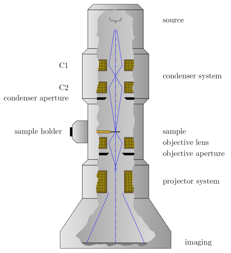
Figure: Schematic cutaway of a TEM (simplified).
Source: http://www.texample.net/tikz/examples/transmission-electron-microscope/
Several of the components of the SEM are similar to the TEM, including the electron source and the acceleration/focusing optics (though one key difference is the typical electron energy used in the SEM, which is 10X or lower than that used in TEM). The components that are unique to the SEM are:
These control the deflection of the electron beam, causing it to scan or raster over the sample at a high rate.
Two types of electrons are used for imaging in SEM, secondary and backscattered. Secondary electrons are relatively low-energy electrons which are produced from interactions between the primary electron beam and the sample.
Backscattered electrons are deflected from the primary beam back towards the source. Secondary electrons are used for generating topographical images of the sample.
The intensity of backscattered electrons depends on the atomic mass of the sample, so images generated from backscattered electrons are said to have Z-contrast. Secondary and backscattered electrons require different detectors because their energy and direction of emission are different.
As with any lab analysis, the first step to using electron microscopy is to develop a plan and set of goals for the analysis. One way of doing this is to list the questions you hope to answer using this technique.
For SEM, the steps commonly followed are:
In TEM, the steps for analysis are similar. However, the process of sample preparation is usually much more difficult and complex. The analysis of the images from a TEM can also be more involved, and for these reasons, TEM analysis is usually performed with the assistance of a trained expert.
As discussed above, a key feature of electron microscopes is that they are used in vacuum. This prevents the analysis of materials which release vapors or would otherwise compromise the vacuum.
In ESEM, the specimen chamber is isolated as much as possible from the sensitive components of the microscope using plates with small apertures for the electron beam, so that a much higher pressure can be maintained in the specimen chamber.
An additional advantage to this type of SEM is that the gas in the specimen chamber is partially conductive, so metallic coatings are not needed on insulating samples.
Another limitation of electron microscopes is their inability to image liquid samples, or particles suspended in liquids. This limitation can be overcome by first freezing specimens to liquid nitrogen temperatures or below, then sectioning them (in the case of TEM), then mounting them cold into the microscope and maintaining their low temperature with specially designed sample holders. This technique is especially useful for imaging complex molecules and biological samples.
In this version of TEM, rather than using a wide electron beam to image the analysis area in parallel, a fine electron beam is rastered across the sample area. This, in combination with continuous improvements in electron optics, has driven a significant improvement in the resolution of electron microscopes[4].
In addition to imaging a specimen, in TEM, an electron diffraction pattern can also be collected, simply by adjusting the focusing optics. This can be useful in determining microstructure of a material, since the electron diffraction pattern can be analyzed to determine the intermolecular or interatomic spacing, and, for crystalline materials, the crystal structure and orientation[5].
In electron microscopy, the interaction of the electron beam with the sample can cause the release of photons. The energy of the photons released is partly a function of the composition of the sample.
In EDS, the energy spectrum of the photons emitted is measured by a detector, and position and intensity of the peaks in this spectrum can be deconvoluted to determine the approximate composition of the sample, or even to map the composition.
Modern EDS analysis software is used to detect the presence of individual elements by automatically detecting and assigning peaks in the EDS spectrum.
However, because EDS peaks are broad, and because multiple elements can have similar EDS peak positions, the operator should manually constrain and double-check the automated analysis. For example, the presence of moderate or high concentrations of exotic elements can usually be ruled out.
EELS is another technique that can be used to determine the composition of the analyzed material, however, it uses the energy lost by electrons in the primary beam as they interact with atoms in the sample in TEM. The main advantage to EELS is that it can be extremely area-specific, even to the point of resolving atomic-scale composition.
Electron microscopes are expensive and sensitive pieces of equipment, so in most cases, they are owned and maintained by trained staff. For the individual users of an electron microscope, there are a number of guidelines that will help to prevent damage to the equipment:
The strength of electron microscopes is primarily their magnifying power, which is several orders of magnitude better than optical (light) microscopes.
Compared to scanning probe microscopes, such as atomic force and scanning tunneling microscopes, they are limited in surface sensitivity, but are more versatile in terms of the types of samples they are able to analyze.
Another strength of electron microscopes is their ability to simultaneously collect composition information in addition to imaging, which is not common in other types of microscopes.
The most commonly encountered drawback of electron microscopes is the sample preparation required, for example cross-sectioning, cleaning, freezing, thinning, and/or coating the sample with a thin layer or metal.
Furthermore, the requirement of running the analysis in vacuum prevents the analysis of certain types of samples (wet biological samples, for example), except when specialized equipment is available.
The complexity and expense of electron microscopes also usually means that they are not as readily available, and can be costly to use. These factors make them generally less versatile compared to light microscopes.
Get the entire package for up to 50% discount with our Replication program.
DISCLAIMER: ConductScience and affiliate products are NOT designed for human consumption, testing, or clinical utilization. They are designed for pre-clinical utilization only. Customers purchasing apparatus for the purposes of scientific research or veterinary care affirm adherence to applicable regulatory bodies for the country in which their research or care is conducted.