
Scanning Tunneling Microscopy, or STM, is a scanning probe technique. This means that the specimen is imaged by scanning a very sharp tip over its surface, while information about the shape or composition of the surface is collected based on interactions between the tip and the sample. This is unlike optical or electron microscopy, where a beam of light or electrons either passes through or reflects off the specimen.
The main advantage of scanning probe techniques is that they are extremely sensitive to height or composition variations on the surface, with some having the potential for even atomic-level resolution (< 0.1 nanometer). In fact, STM was the first technique which was able to distinguish individual atoms on a surface.[1] Its inventors were awarded the Nobel Prize in physics in 1986.
In STM, the interaction between the probe tip and the specimen consists of quantum tunneling of electrons. This is a process where electrons can cross over a barrier, in this case the empty space between the specimen and the probe.
This is because the location of an electron is not described by a fixed position, but by a cloud, where the electron may exist anywhere within the cloud. If the cloud of an electron extends across a barrier, the electron can cross over it by existing simultaneously on both sides of the barrier.
Electron tunneling can happen at distances < 3 nm, with a probability that is strongly dependent on distance, which gives STM its extreme sensitivity at short length scales.
This is a simplified explanation, and a full analysis of tunneling in specific cases requires determining the quantum wavefunction of the electron in the system,[2] through use of the Schrӧedinger equation or other formulations.
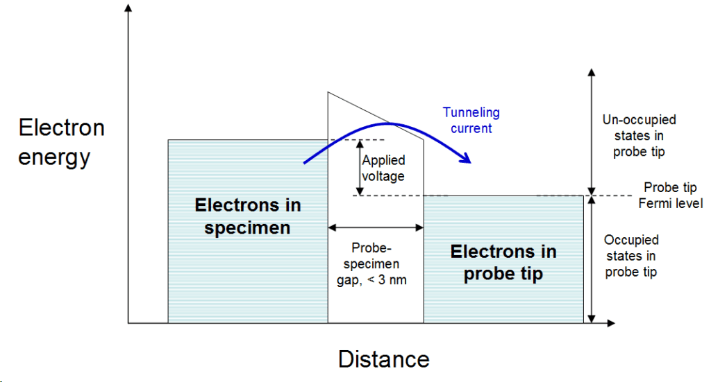
Electrons can tunnel either between the tip and the specimen, or vice versa, depending on the applied voltage. In either case, the rules of quantum tunneling require that the individual electron tunnels between an occupied energy state in one to the same, unoccupied state in the other.
A central idea in quantum physics is that electrons exist in materials in such discrete (or quantized) energy states. The process of tunneling is shown schematically in the figure below.

Figure: Schematic of the tunneling process.
The rate that electrons cross the barrier (or the tunneling current) depends on:
Tunneling current is roughly proportional to the first two, and depends exponentially on the third.[3]
In this article, we will first describe the various types of analysis that can be done with STM, based on the dependence of tunneling on these three factors. We will then discuss practical aspects of STM, including the parts of a typical STM setup, and considerations when performing experiments with an STM.
The three parameters that the STM analyst can vary and/or measure are the applied probe to specimen voltage, the probe height, and the tunneling current.[4] A number of different techniques can be built by varying these parameters. They are described below, from simplest to most complex.[5]
In this simple model, the probe is scanned (or rastered) in the x and y directions across the specimen. While the tip is being rastered, a voltage is applied to the specimen and the resulting tunneling current is measured.
An electronic feedback loop attempts to then keep this tunneling current constant during the x-y scanning by adjusting the z-position (height) of the probe tip. For example, if the tunneling current is higher than the set value, the feedback loop will retract the tip. Typical scan areas are in the ~ 100 to 10,000 nm2 range.
The resulting information is a two-dimensional x-y map of the probe height required to maintain a constant tunneling current, sometimes called a “topographic” map.
This height is a combination of the physical height variation of the surface, and the local density of electron states. The very strong exponential dependence of tunneling current on probe-specimen distance, however, results in high sensitivity to surface topography.
This mode is similar to the constant tunneling current mode, except that the tunneling current is measured, and the height of the probe tip is held constant.
The result in this case is a map of the tunneling current at constant height. As with constant current mode, the magnitude of the tunneling current depends on the shape of the surface, and the density of electron states.
The main advantage to constant height STM is that the tip can be scanned faster, since no feedback is needed. However, it requires an atomically flat specimen, and can only be used over small areas, since without feedback there is danger of having the probe contact the specimen.
A more sophisticated form of STM analysis involves varying or modulating either the probe to sample distance, or the applied voltage, during an x-y scan.
In the first case, the change in the tunneling current with probe to sample distance (dI/dz) is proportional to the local work function of the specimen.
The work function is the amount of energy required to remove an electron from a material, and depends on the composition and structure of the surface just under the probe tip.
In the second case, the change in tunneling current with applied voltage (dI/dV) is proportional to the local density of states in the material. So scanning in x-y while modulating the applied voltage can be used to map the density of states in the material, another useful diagnostic tool.
In the techniques of barrier height and density of states mapping, the height or voltage are continuously modulated during the x-y sweep. A more comprehensive analysis can be done where the probe stops at each point in the x-y scan, and runs a full sweep of probe height or supply voltage, measuring the resulting tunneling current response.
These are full I vs. Z and I vs. V curves. This type of scanning is much slower, but results in a full spectroscopic data set at each point, which can be useful when the response of the specimen is not easy to predict.

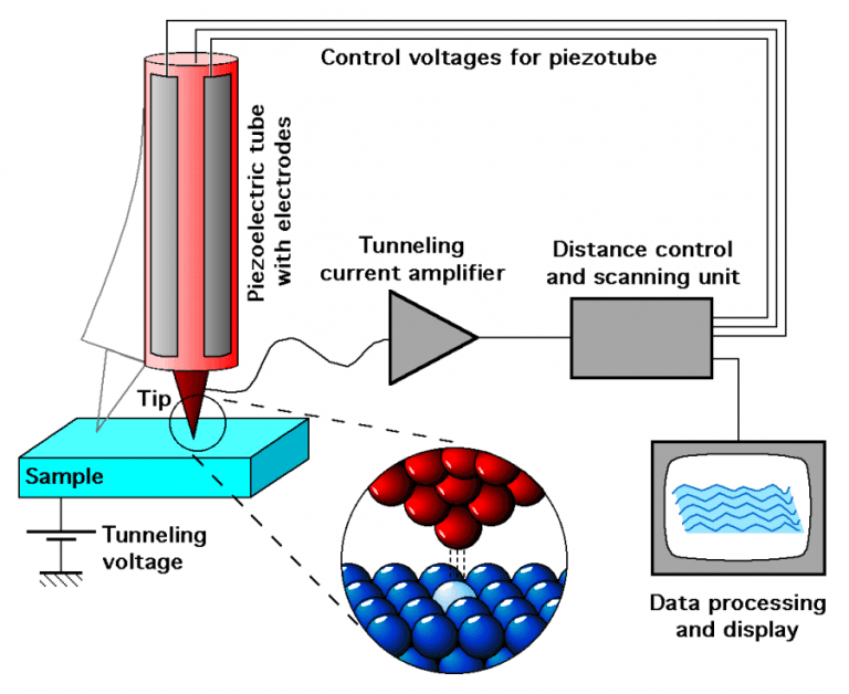
Figure: Schematic of an STM system.
Source: http://www.iap.tuwien.ac.at/www/surface/stm_gallery/stm_schematic
The probe tip is a critical part of the STM because it directly interacts with the specimen. The most critical aspect of the probe is the sharpness of the tip itself, which effectively determines the resolution of the image.
STM probes are traditionally metallic, specifically, either tungsten or platinum-iridium are common. They are formed by either mechanical methods, like shearing, or by electrochemical etching.[6] More recently, carbon nanotubes have been used.
The position of the tip in all three dimensions is typically controlled using piezoelectric transducers,[7] or simply “piezos”. These consist of crystals that expand or contract by minute amounts when voltage is applied. So by applying variable voltages to crystals controlling the x and y positions, the position of the probe tip can be scanned across the specimen.
Conversely, if the piezo crystals are compressed or put in tension, a voltage is generated across the crystal. So the position of the probe tip can also be sensed by measuring the voltage.
In an STM setup, the piezo crystals responsible for x and y motion are directly controlled by a computer. Z motion, which determines the probe height, has the additional capability or being controlled by a feedback loop in constant tunneling current measurements.
The electronics in an STM are straightforward but very sensitive and precise. First, a voltage source applies a small voltage to the specimen. When the probe is at a typical scanning distance (< 1 nm, or 10-9 m), a small tunneling current, on the order of 10-9 A, is generated. An amplifier converts this small current to a voltage, and this voltage signal is sent to control electronics.
Unlike electron microscopy, there is nothing inherent about the physics of the STM technique that requires special environmental conditions. However, since STM is surface-sensitive, a highly controlled environment is required to maintain surface cleanliness.
Consider that at 10-6 Torr, considered a moderately high vacuum, a gas molecule impacts every atom on a surface once per second. For that reason, STM analysis is normally performed under ultra-high vacuum conditions, which greatly reduces contamination from background gases.
However, STM can be performed in other controlled environments, including under the surface of liquids.[4]
Because the distances being measured in STM are extremely small, at times < 0.1 nm, the technique is very sensitive to vibrations, even more so than other microscopy techniques.
Even the imperceptible vibrations from a nearby road or other lab equipment can severely limit or even prevent the operation of an STM. For that reason, all components in the STM are designed to be rigid.
Furthermore, STM equipment must be isolated from vibrations by mounting it on dampening air springs or similar hardware. The placement of the STM in a building is also critical for this reason.
Analysis using STM is normally done with the assistance of a trained expert since these instruments are extremely sensitive and complicated to operate. Similar to TEM, one of the most difficult and critical aspects of the process is sample preparation. The quality of the analysis often depends on how well the sample was prepared.
Analysis by STM is highly dependent on the type of sample and the instrument being used. The steps given here are a rough generalization of the analysis method.
Scanning tunneling microscopes are expensive and sensitive pieces of equipment, so in most cases, they are owned and maintained by trained staff. For the individual users of an STM, there are a number of guidelines that will help to prevent damage to the equipment:
Scanning tunneling microscopes are quite different from the more common optical and electron microscopes, and the information they provide is different and often complementary to those instruments.
STM differs from those techniques mainly in its ability to provide detailed information on the atomic-level, local structure of the surface of a material, and extremely good resolution in the vertical (height) dimension. Because of this, STM is considered a surface science tool as well as a microscope.
STM is closely related to atomic force microscopy (AFM), which is also a scanning probe technique with good height resolution. The key difference between STM and AFM is that AFM uses intermolecular or interatomic forces, rather than quantum tunneling, to scan the surface.
The main drawbacks to STM are:
