x
[quotes_form]

Microfluidic Chips

See more by:

$750.00$1,200.00

10% off with your subscription Membership
 / Availability: In Stock / Delivery Info ⓘ

Description

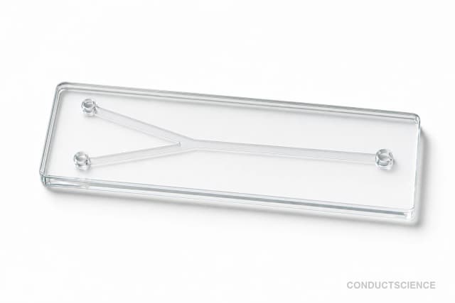
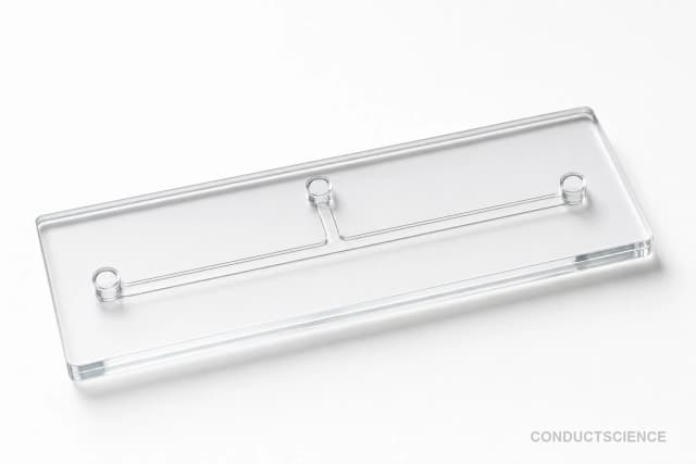
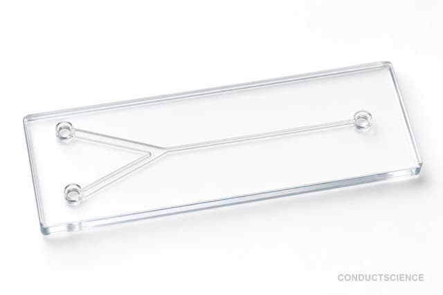
Our microfluidics chips are designed specifically for life science applications. This advanced chip technology enables precise control of fluidic flow, allowing for highly accurate analysis and manipulation of biological samples. With its compact size and ease of use, our microfluidics chip is perfect for a range of applications, including single-cell analysis, drug discovery, and protein crystallization. Whether you’re a researcher, scientist, or engineer, our microfluidics chip is the ideal tool for advancing your life science research.

Microfluidic chips are made from either glass or polymethyl methacrylate (PMMA) and can be etched to your custom specifications.

ConductScience offers Custom Microfluidic Chips.

Please contact us prior to ordering

Meet the producer

Producer:

Frequently bought together

More from this Producer

Description

Microfluidic chips are made from either glass or polymethyl methacrylate (PMMA) and can be etched to your custom specifications. Microfluidic chips are gaining traction in scientific research for use in projects  such as:


  1. “Mazes” for immune, bacterial, and parasitic cells
  2. Organ / body / tumour system-on-a-chip
  3. Biomarker analysis
  4. Droplet and liquid mechanical analysis 
  5. Optical research 
  6. Diagnostics 
  7. Biosensors 
  8. Particle analytics 


Resistant to high temperatures, pressures, and corrosion with heat performance capabilities, our microfluidic chips can be used for a wide variety of scientific purposes.

Introduction

A microfluidic chip comprises an incorporated pattern of microchannels linked to the macro-environment via several holes hollowed out through the chip. Fluids are injected into and out of the microfluidic chips through these holes. Fluids are mixed, separated, directed, or manipulated to attain automation, multiplexing, and highly efficient systems. The microchannel network design should be precisely explained to achieve desired features like pathogen detection, lab-on-a-chip, electrophoresis, DNA analysis, etc. 

Microfluidic technology was first introduced in the 1990s and has experienced a significant evolution since then (Scott and Ali, 2021). Microfluidic devices that can handle very minute amounts of fluids for medical, biological, and chemical applications are developing rapidly. Microfluidic chips can have microchannel dimensions of up to a hundred microns that can handle micro volumes ranging from 1 attolitre to one nano-liter. 

Microfabrication 

Microfluidic chips can be fabricated from a variety of materials, including silicon, quartz, or glass. The ‘fabrication’ process involves the formation of channels on a solid substrate’s surface followed by drilling holes into the substrate, ultimately bonding it to another plate to seal the channels.  Tubing/reservoirs are then connected to the access holes, facilitating the introduction of solutions. Earlier, microfluidic devices were fabricated via photolithography and wet etching methods. Polymer chips are popular due to their amenability to mass fabrication. Apart from glass, silicon, and quartz, flexible elastomer poly-dimethylsiloxane (PDMS) is the most employed chip material in research labs. PDMS is appropriate for prototyping.  Sometimes, the microchannel surfaces are modified by several techniques like organosilane deposition to display the characteristics of specific functional groups. 

The progress in microfluidic technology is firmly attributed to microelectronics requirements. Silicon wafers are the dominant substrate type and will continue to form the basis of microfluidic chips. Silicon patterning in microfluidic devices employs anisotropic wet etching or dry etching by reactive ion etching (RIE) and deep reactive ion etching (DRIE). Quartz or glass patterning typically utilizes wet iron etching by hydrofluoric acid (HF). These microfluidic processes can be employed for MEMS (Micro-electromechanical Systems) fabrication, sensors, or optoelectronic devices. Following are some basic microfabrication techniques. 

  • Lithography

Lithography is the process used to transfer 3D patterns onto a surface. It is the most significant step in the microfabrication process as the definition of the shape of elements constituting the device is performed here. A general lithographic process follows the underlying steps.

  1. Designing the pattern
  2. Forming the mask 
  3. Coating the wafer
  4. Exposing the photoresist 
  5. Developing the photoresist

Photolithography, also referred to as UV lithography principally uses UV light through a photomask or hard mask to expose the PR (photoresist). “Photoresist is a light-sensitive polymeric solution.” Negative photoresists are the regions that are insoluble in the developer on exposure to light. They generate a minimum feature size of 2 µm and a spreading thickness of 1-3µm. On the contrary, positive PR are the regions that become soluble in developer on exposure to light and have m.f.s of up to 1 µm and spin-coated spreading thickness from 1.5-7µm. 

A geometric pattern is designed using a computer-aided design (CAD), which is then transferred to a light-sensitive polymer known as photoresist (PR), previously spin-coated on a substrate, by exposing the substrate to a light source like UV, Laser, or electronic beam. The light passes through a hard mask/photomask to expose the PR, or it can be maskless, as in the case of laser lithography. Following PR development, the substrate can proceed to the next step. 

The photoresist is exposed to light for a given duration and energy, predetermined by energy adsorption. Laser lithography is a lithographic technique in which laser light is used to fabricate large precision patterns. The minimum feature size achieved with this technology is 0.8µm or less and depends on the laser wavelength and optical path. Moreover, we can modulate the laser intensity, partially exposing the photoresist. This method is known as Laser direct with grayscale photolithography. It creates microscale features with multilevel topography. The photomask is usually defined on a thin metallic film layer such as aluminum, chromium, etc., opaque to UV light, and deposited on a flat UV-transparent substrate. The computer-automated design of geometric patterns provides increased definition and is defined over large-sized substrates of up to 30cm.

Additionally, the exposure strategy will determine process resolution, limited by diffraction. For instance, in contact lithography, the photomask is in direct contact with the photoresist. The features to be transferred are at zero magnification to achieve a minimum feature size (m.f.s) of 0.5 µm. The technique is quite simple and inexpensive. However, direct contact with the mask can smear or degrade features, causing loss of sharpness. 

Exposure techniques where the mask is not in direct contact are proximity printing (a minute gap between PR and mask with a 1:1 magnification) or projection printing (projection from a distance and a demagnification of 1:4- 1:10 or even lower). In proximity printing, diffraction limits the pattern transfer repeatability and accuracy, and the resolution worsens by 1-2µm. The optical path determines the resolution in projection printing, which can attain a minimum feature size of approximately 0.065 µm and is the most expensive of the three. 

The minimum feature size magnification (m.f.s) used is determined by the PR type used in the process. Following exposure, the PR is developed to remove unwanted regions. The resolution and definition of microfabricated patterns depend on development time and conditions (temperature, concentration, agitation, etc.). The photoresist still presents on the substrate will determine whether the etching regions or deposition regions remove or add material in a consequent fabrication step. 

  • Subtractive Techniques for Pattern Transfer Microfabrication

The subtractive techniques for microfabrication include etching methods involving physical or chemical removal of the material. Generally, it employs two approaches, i.e., dry etching (using plasma methods) and wet etching (using chemical solutions). Additionally, the reactive ion etching (RIE) method is frequently used, a combination of the above two.

 Wet Etching

Wet etching is the use of liquid etchant to remove material from any substrate. Wet etching can be isotropic or anisotropic

In isotropic etching, the surface material is uniformly in all directions of the chemical structure. It is orientation-dependent and uses aqueous acidic solutions containing HF and azanone (HNO), or HNO (mixture of hydrofluoric acid, nitric acid, and acetic acid) to remove surface material. Process time and homogeneity are affected by factors like agitation and temperature. The substrate composition defines the final etched shape. Isotropic etching of silicon yields characteristic round corners and is diffraction-limited.  

In anisotropic etching, the surface material removal depends on the crystalline structure orientation of the surface. It employs crystal-orientation etchants of silicon such as alkali metal hydroxides (KOH, NaOH, RbOH, CEO). The rate of wet etching is enhanced by tuning agitation and temperature. Moreover, wet etching produces limited microchannel geometries, limited by wafer type and orientation. It is a simple, robust, and cost-effective etching technique.

Dry Etching

Dry etching uses plasma or etchant gases to remove material from any surface at low temperatures (room temperature to 250oC) and low pressure (a few millitorrs). The reactions occur in the presence of high-energy particle beams like electron or proton beams to etch substrate atoms. This process is called physical dry etching. Additionally, chemical reactions between etchants attack the substrate in chemical etching. The technique involves the use of dry gases like CH4, SF6, Cl2, and F2. Both processes can be combined to achieve higher resolution in a process, reactive ion etching (RIE). RIE is the most extensively used process in research laboratories and industries. Typically, gases for silicon substrates in RIE are CF6, SF6, and BCl2 + Cl2

Deep Reactive Iron Etching (DRIE)

Deep reactive ion etching (DRIE) is a recently developed technique that facilitates in-depth features of several hundreds and thousands of micrometers into a substrate with nearly vertical walls. It enables high aspect ratio elements to be defined into silicon, metal, or glass substrates. 

The Bosch etch is the most frequently used technique on a commercial basis. In this technique, deep vertical walls with a characteristic scalloped sidewall typically with a peak-to-peak roughness of about 0.3 µm. It needs laser lithography to outline a PR mask that defines the unprotected areas to be etched. Although time-consuming and costly, the technique presents low manufacturing uncertainty. Additionally, this method can synthesize unlimited geometries and helps attain m.f.s of a few micron meters.  

  • Additive Techniques for Pattern Transfer

The additive microfabrication technique involves the mechanical, chemical, or thermal addition of materials, usually selectively, to a substrate. 

Physical Vapor Deposition (PVD) is the most familiar fabrication material used for microfluidic chips. The technique involves depositing thin films onto the substrate by the material’s condensable vapor to deposit through low pressure or vacuum gaseous environment. Techniques like sputtering, thermal evaporation, ion plating, aerosol deposition, laser ablation, etc., are used to shift the vapor from the target source to the rigid substrate. Additive microfabrication includes underlying steps:

  1. Synthesizing vapor coating onto the surface of the substrate
  2. Transporting vapor to the substrate
  3. Condensing the vapor coating onto the substrate 

A sputtering deposition involves bombarding a sputtering target with accelerated non-reactive ions in a plasma atmosphere. The ions intruding on the substrate employ the phenomenon of momentum transfer to erode the target. The material ejected from the target becomes condensable vapor for deposition. 

Thermal evaporation mainly incorporates deposition metals or low fusion temperature compounds using resistive or electron beam heating. Unlike sputtering, evaporation provides directional deposition from the source and presents poor sidewall coating compared to surface coating. Moreover, this method has lower deposition rates at higher substrate temperatures than sputtering, consequently forming thin films with high tensile stresses. 

Surface micromachining involves the fabrication of micromechanical structures from thin films deposited on the silicon substrate. A thin-film deposition is a technique in which layers of thin films are added to the substrate surface. Surface micromachining is used in combination with wet etching as a fabrication method for a cantilever. In this technique, a thin film that acts as a temporary mechanical layer (sacrificial layer) is deposited on which subsequent device layers are built. Following this, the deposition and patterning of the structural layer of the thin film occur. Finally, the etching of the sacrificial layer is done that is ultimately followed by the release of a cantilever, aiding the polysilicon structural, and mechanical layer to move (Silverio and Freitas, 2018).  

  • Polymer-based Microfabrication Techniques

Polymeric materials are used as cheaper and easier microfabrication solutions in biological detection processes. These are easily replicable, biocompatible, and have appropriate thermal and electrical properties. Two important polymers used in this regard include elastomers and thermoplastics. 

Elastomers 

The most used elastomer in the rapid prototyping of microfluidic devices is PDMS. The PDMS is cast and cured onto a microscale mold and sealed onto a wide variety of materials. PDMS comprises a two-part heat-curable mixture. The pre-polymer is cross-linked with a curing agent with a 10:1 ratio in weight. One can alter the chemical and physical properties of the mixture by changing this ratio. Microfabrication using PDMS offers benefits like cost-effectiveness, biocompatibility, low toxicity, inertness, mechanical flexibility, durability, and ease of manipulation. The low PDMS stiffness (about 1MPa) accounts for the integration of valves and pumps to generate 3D multilayered devices. PDMS is appropriate for low aspect ratio microchannels. However, channels with a high aspect ratio are hard to obtain and can collapse. It is susceptible to minute changes in applied pressure, and compression in PDMS structures can lead to cracks in feature dimension deformation. 

The gas and water permeability and hydrophobic nature of PDMS work in favor and against its utility. For instance, non-specific protein/ hydrophobic analytes, cells, or bacteria easily adhere to PDMS walls, whereas in some applications, ill-designed bioanalytes can obstruct the flow, causing device fouling. 

The soft lithography technique rapidly fabricates many elastomeric devices using mechanically soft materials like polymers without costly capital equipment. It is a prolongation of photolithography.

Thermoplastic Polymers

Thermoplastic-based microfluidic chips are becoming popular because of their ease of being produced on a large scale. Moreover, they are cost-effective, allow faster processing, have almost unlimited tailoring and don’t require a clean environment. Thermoplastic characteristics include negligible resistance, biocompatibility, high glass transition temperature, fluorescence, and broadly visible transmittance. However, there might be a few drawbacks depending on the application. For example, some organic solvents may dissolve thermoplastics decreasing their mechanical stiffness. Additionally, they can absorb UV light, thus inhibiting their usage in a variety of applications.   

Bonding

Hybridization is a critical process to assemble different parts of the device into a final product. Microfluid chips require the bonding of several factors to generate confined volumes for fluid manipulation. An extensive range of bonding strengths can be attained based on bonding material and technique. Additionally, bonding requires flat and smooth surfaces to prevent voids between the bonded parts and achieve excellent bonding. It also needs high temperature and high electrical field that might damage electronic elements on the device (Silverio and Freitas, 2018). 

Apparatus and Equipment

Conduct Science offers high-quality, customizable microfluidic chips for pharmaceutical, analytical, industrial, and research purposes that can be designed according to your experimental requirements.

Applications

Pharmaceutical Analysis

Drug development involves processes like drug discovery, preclinical, and clinical trials. All these processes require pharmaceutical analysis. As a miniaturization technology, microfluidics is a powerful tool for rapid screening and analysis of drug discovery. The volume of a microfluidic chip is minimal, and many functions can be integrated on a chip of several centimeters. A microfluidic chip with internal dimensions ranging from micrometers to millimeters is used to sample volume at the nano-liter or pico-liter level.

Microfluidic technology offers excellent benefits in high throughput drug sequencing (HTDS) compared to conventional cell assay systems. These high-throughput techniques are significant for screening pharmacologically valuable lead compounds. Cui and Wang (2019) presented the following different microfluidic chip technologies used in drug screening.

  • Droplet Microfluidics 

Droplet microfluidics utilizes liquid droplets, such as nano- or picoliter-sized droplets, segregated in an immiscible fluid, which are independent reaction vessels to conduct experiments in continuous or segmented flow. The applications of on-chip concentration gradients and multicellular spheroids expanded the range of applications of microdroplets. They simplified the screening process, made the established screening model closer to the human body, and enabled more reliable results. These methods can also be used for drug combination screening based on sequential operation droplet array technique and optimize dosing regimen with minimal consumption, which is a meaningful situation of combined diseases. 

  • Organ-on-Chip

The microscale control of organ structure and flow has enabled the accurate modeling of tissues at the microscale. Organ-on-chips are bio-engineered “biomimetic systems” that simulate functional human organs like the liver, kidney, lungs, and gut. These “in vitro models” facilitate pharmacological modulation and simulation of complicated biological phenomena. Additionally, “body-on-chip” microfluidic chips integrate multiorgan simulation to predict organ interactions. The organ-on-chip approach is also used to study the tumor microenvironment and anti-cancer drug toxicity and effectiveness. 

  1. Three-Dimensional Cell Culture

Three-dimensional tissue models help study cell-cell and cell-extracellular matrix interactions and spatial and physiochemical diversity that profoundly influence diseases. Recently, “high throughput 3D formation platforms” have been developed for drug screening, fabricating cell microarrays, and introducing tumor spheroids to assess anti-cancer drugs and mimic heterogeneous tumor tissues for cytotoxicity testing of these drugs. 

Immunoassay for Breast Cancer Biomarker Detection

Oliveria et al. (2019) described the construction of a disposable microfluidic immunoassay device (DµID) for robust and cost-effective detection of (CA15-3) carbohydrate antigen 15-3, a protein biomarker for breast cancer. The first step was the fabrication of a screen-printed electrode array. Microfluidic immunoassay was constructed using 8 disposable electrodes, 1 counter electrode, and 1 reference electrode. First, the immunoassay was designed using software, and then its pattern was transferred onto an adhesive vinyl film using a cutter printer. Following this, the researchers removed unwanted parts using tweezers to form a mask of electrode patterns. Then they placed the vinyl film over the polyester sheet having dimensions 21.0 x 29.7cm. Then, applied a carbon sheet on top of the sheet and used a squeegee to fill electrode patterns with ink. They cured the ink for 30 minutes at 60oC and removed the vinyl mask. They delimitated the geometric area of 8 working electrodes by cutting a vinyl mask with 8 holes of 2mm diameter using a cutter printer and placed it, thus forming microwells. A heat press was used for better adhesion, and silver/silver chloride ink was applied over the reference electrode using a brush and cured at 60oC for half an hour. Once ready, they made two holes for the inlet and outlet. 

The second step was the preparation of the immunosensor and fabrication of DµID. The scientists modified the screen-printed electrode array with an Ab1 mouse monoclonal antibody, and once it was ready, they used the immunoassay to assemble DµID. They used a double-sided polystyrene adhesive to synthesize microchannels using a cutter printer, removed the adhesive protective film, and applied the card onto the immunoarray. Moreover, they spread the other layer with reference and counter electrode with holes for the inlet and outlet and pressed it using a heat press. Once ready, the device was stored at 4oC. The system was assembled by connecting to the syringe pump, injector valve, and multipotentiostat.  Method parameters were optimized, and offline biomarker capture was followed by online DµID detection. They used DµID for the detection of CA15-3 in actual cancer patient samples and obtained excellent detection results. 

Genetic Analysis 

Microfluidic chips for DNA and RNA are widespread. Microscale PCR uses aqueous droplets in oil as micro-reaction vessels for individual DNA molecules referred to as “digital droplet PCR” which can be constructed on a microfluidic chip. Microfluidic chips can be used for single-cell PCRs and nucleic acid isolation. Wu et al. (2016) implemented single-cell PCR on a microfluid chip to explore the cellular composition of normal human colon and colon cancer epithelia. They also combined PCR with microchip electrophoresis to analyze the BCR-ABL fusion gene. They employed a microfluidic chip with 3×3 arrayed electrochemical sensors for analyzing DNA hybridization events. They also used these chips to analyze the mRNA levels in “enriched tumor exosomes” harvested from blood to monitor the level change during treatment. In a nutshell, these chips provide a comprehensive genetic screening platform for research and analysis.

Strengths and Limitations

Microfluidic chips present considerable advantages such as reduced sample consumption, enhanced reaction speed, increased reliability and reproducibility, biocompatibility, and manipulation of minimal volumes with flexible composition control. Compared to conventional 96-well techniques used for drug screening, microfluidic chips require approximately 200 times low sample volumes and offer reduced reaction time due to an increased surface-volume ratio. Additionally, a cost-effective slip chip presents an accessible and commercially viable method for carrying out microfluidic reactions without pumps and valves (Cui and Wang, 2019).  

However, there are a few limitations associated with the conventional fabrication of microfluidic chips, for instance, high per unit area substrate cost and lengthy, time-consuming processes including cleaning, patterning, etching, and deposition steps. Moreover, the specific physical properties of traditional materials are undesirable. For example, silicon being an electrical conductor can present problems for electro-osmotic pumping. Similarly, quartz and glass require high temperatures and voltage for bonding (Scott and Ali, 2021). 

Summary

  • A microfluidic chip comprises an incorporated pattern of microchannels that are linked to the macro-environment via several holes hollowed out through the chip.
  • Microfluidic chips can be fabricated from a variety of materials, including silicon, quartz, or glass. The ‘fabrication’ process involves the formation of channels on a solid substrate’s surface followed by drilling holes into the substrate, ultimately bonding it to another plate to seal the channels.
  • Lithography, dry etching, wet etching, and polymer-based microfabrication methods can be used.
  • Lithography is the process used to transfer 3D patterns onto a surface. This is the most significant step in the microfabrication process as the definition of the shape of elements constituting the device is performed here.
  • Wet etching is the use of liquid etchant to remove material from any substrate. Wet etching can be isotropic or anisotropic.
  • Dry etching uses plasma or etchant gases to remove material from any surface at low temperature (room temperature to 250oC) and low pressure (few millitorrs).
  • Deep reactive ion etching (DRIE) is a recently developed technique that facilitates in-depth features of several hundreds and thousands of micrometers into a substrate with nearly vertical walls.
  • Polymeric materials, including elastomers and thermoplastics, are cheaper and easier microfabrication solutions in biological detection processes.
  • Microfluidic chips have extensive applications in pharmaceutical analysis, drug development, immunoassay for biomarker detection, anti-cancer drug analysis, and biomolecular analysis.

Additional information

Product Qty

5, 10, 15, 30

Brand

ConductScience

Product Application

Drug discovery, Point-of-care diagnostics, Protein crystallization, Single-cell analysis

Field of study

Agriculture, Biochemistry, Biomedical Engineering, Chemistry, Food Science, Microelectronics, Molecular Biology

Reviews

There are no reviews yet.

Be the first to review “Microfluidic Chips”

Questions & Answers

There are no questions yet. Be the first to ask a question about this product.

Want to ask a question or need information? Fill in the form and contact us directly